
. DOI: 10.1038/s44306-023-00003-2")
Researchers at Tohoku College have developed pointers for a single-nanometer magnetic tunnel junction (MTJ), permitting for efficiency tailoring to satisfy the necessities of various functions, starting from AI/IoT to cars and area applied sciences.
The breakthrough will result in high-performance spintronic non-volatile reminiscence, appropriate with state-of-the-art semiconductor applied sciences. The small print have been revealed within the journal npj Spintronics on January 4, 2024.
The important thing attribute of non-volatile reminiscence is its capability to retain knowledge within the absence of an exterior energy supply. Consequently, in depth growth efforts have been directed in the direction of non-volatile reminiscence due to its capability to scale back energy consumption in semiconductor built-in circuits (ICs). Efficiency necessities for non-volatile reminiscence differ in accordance with particular functions. For example, AI/IoT functions demand high-speed efficiency, whereas automotive and area applied sciences prioritize excessive retention capabilities.
Spin-transfer torque magnetoresistive random entry reminiscence (STT-MRAM), a kind of non-volatile reminiscence know-how that shops knowledge by using the intrinsic angular momentum of electrons, often known as spin, possesses the potential to deal with a number of the limitations related to current reminiscence applied sciences.
The fundamental constructing block of STT-MRAM is the magnetic tunnel junction (MTJ): two ferromagnetic layers separated by a skinny insulating barrier. Scientists have lengthy tried to satisfy the problem of creating MTJs smaller whereas assembly efficiency necessities, however many issues stay.
STT-MRAM, using MTJs with dimensions within the vary of a number of tens of nanometers, has been efficiently developed for automotive semiconductors utilizing 1X nm know-how nodes. Waiting for future nodes, nonetheless, there’s a have to scale down MTJs to single-digit nanometers, or X nm, whereas guaranteeing the potential to tailor efficiency in accordance with particular functions.
. DOI: 10.1038/s44306-023-00003-2")
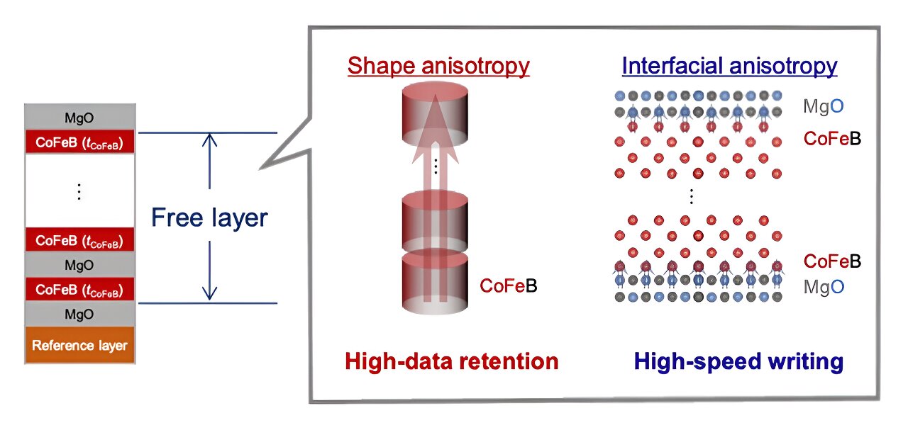
To do that, the analysis group designed a method to engineer single-nanometer MTJs with a CoFeB/MgO stack construction, a de facto commonplace materials system. Various the person CoFeB layer thickness and the variety of [CoFeB/MgO] stacks allowed them to regulate the form and interfacial anisotropies independently—one thing essential for reaching high-retention and high-speed capabilities, respectively.
Consequently, the MTJ efficiency might be tailor-made for functions starting from retention-critical to speed-critical. On the dimension of single nanometers, shape-anisotropy enhanced MTJs demonstrated excessive retention (> 10 years) at 150°C, whereas interfacial-anisotropy enhanced MTJs achieved quick pace switching (10 ns or shorter) under 1 V.
“For the reason that proposed construction might be tailored to current amenities in main semiconductor factories, we consider that our research gives a major contribution to the longer term scaling of STT-MRAM,” stated Junta Igarashi, one of many lead authors of the research.
Principal Investigator Shunsuke Fukami added that “Semiconductor industries usually are usually aware of long-lasting scaling. In that sense, I feel this work ought to ship a powerful message to them that they will depend on the way forward for STT-MRAM to assist usher in a low-carbon society.”
Extra data:
Junta Igarashi et al, Single-nanometer CoFeB/MgO magnetic tunnel junctions with high-retention and high-speed capabilities, npj Spintronics (2024). DOI: 10.1038/s44306-023-00003-2
Supplied by
Tohoku College
Quotation:
Tips for single-nanometer magnetic tunnel junction know-how (2024, January 17)
retrieved 17 January 2024
from https://phys.org/information/2024-01-guidelines-nanometer-magnetic-tunnel-junction.html
This doc is topic to copyright. Other than any honest dealing for the aim of personal research or analysis, no
half could also be reproduced with out the written permission. The content material is offered for data functions solely.
