
There was a time, many years actually, when all it took to make a greater pc chip have been smaller transistors and narrower interconnects. That point’s lengthy gone now, and though transistors will proceed to get a bit smaller, merely making them so is now not the purpose. The one strategy to sustain the exponential tempo of computing now could be a scheme referred to as system expertise co-optimization, or STCO, argued researchers at ITF World 2023 final week in Antwerp, Belgium. It’s the power to interrupt chips up into their purposeful parts, use the optimum transistor and interconnect expertise for every operate, and sew them again collectively to create a lower-power, better-functioning entire.
“This leads us to a brand new paradigm for CMOS,” says Imec R&D supervisor Marie Garcia Bardon. CMOS 2.0, because the Belgium-based nanotech analysis group is asking it, is a sophisticated imaginative and prescient. However it could be essentially the most sensible approach ahead, and components of it are already evident in at present’s most superior chips.
How we acquired right here
In a way, the semiconductor business was spoiled by the many years previous to about 2005, says Julien Ryckaert, R&D vp at Imec. Throughout that point, chemists and gadget physicists have been capable of often produce a smaller, lower-power, quicker transistor that may very well be used for each operate on a chip and that might result in a gentle enhance in computing functionality. However the wheels started to return off that scheme not lengthy thereafter. System specialists may provide you with glorious new transistors, however these transistors weren’t making higher, smaller circuits, such because the SRAM reminiscence and customary logic cells that make up the majority of CPUs. In response, chipmakers started to interrupt down the obstacles between customary cell design and transistor improvement. Known as design expertise co-optimization, or DTCO, the brand new scheme led to units designed particularly to make higher customary cells and reminiscence.
However DTCO isn’t sufficient to maintain computing going. The boundaries of physics and financial realities conspired to place obstacles within the path to progressing with a one-size-fits-all transistor. For instance, bodily limits have prevented CMOS working voltages from lowering beneath about 0.7 volts, slowing down progress in energy consumption, explains Anabela Veloso, principal engineer at Imec. Transferring to multicore processors helped ameliorate that subject for a time. In the meantime, input-output limits meant it turned increasingly more essential to combine the features of a number of chips onto the processor. So along with a system-on-chip (SoC) having a number of cases of processor cores, in addition they combine community, reminiscence, and sometimes specialised signal-processing cores. Not solely do these cores and features have totally different energy and different wants, in addition they can’t be made smaller on the similar fee. Even the CPU’s cache reminiscence, SRAM, isn’t cutting down as rapidly because the processor’s logic.
System expertise co-optimization
Getting issues unstuck is as a lot a philosophical shift as a set of applied sciences. In line with Ryckaert, STCO means taking a look at a system-on-chip as a set of features, akin to energy provide, I/O, and cache reminiscence. “If you begin reasoning about features, you notice that an SoC just isn’t this homogeneous system, simply transistors and interconnect,” he says. “It’s features, that are optimized for various functions.”
Ideally, you would construct every operate utilizing the method expertise finest suited to it. In apply, that principally means constructing every by itself sliver of silicon, or chiplet. Then you definitely would bind these collectively utilizing expertise, akin to superior 3D stacking, so that every one the features act as in the event that they have been on the identical piece of silicon.
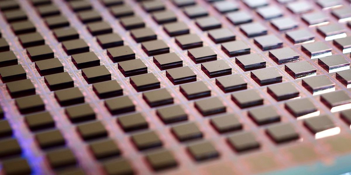
Examples of this pondering are already current in superior processors and AI accelerators. Intel’s high-performance computing accelerator Ponte Vecchio (now referred to as Intel Knowledge Heart GPU Max) is made up of 47 chiplets constructed utilizing two totally different processes, every from each Intel and Taiwan Semiconductor Manufacturing Co. AMD already makes use of totally different applied sciences for the I/O chiplet and compute chiplets in its CPUs, and it just lately started separating out SRAM for the compute chiplet’s high-level cache reminiscence.
Imec’s highway map to CMOS 2.0 goes even additional. The plan requires persevering with to shrink transistors, transferring energy and probably clock indicators beneath a CPU’s silicon, and ever-tighter 3D-chip integration. “We are able to use these applied sciences to acknowledge the totally different features, to disintegrate the SoC, and reintegrate it to be very environment friendly,” says Ryckaert.
 Transistors will change type over the approaching decade, however so will the steel that connects them. Finally, transistors may very well be stacked-up units made from 2D semiconductors as a substitute of silicon. Energy supply and different infrastructure may very well be layered beneath the transistors.Imec
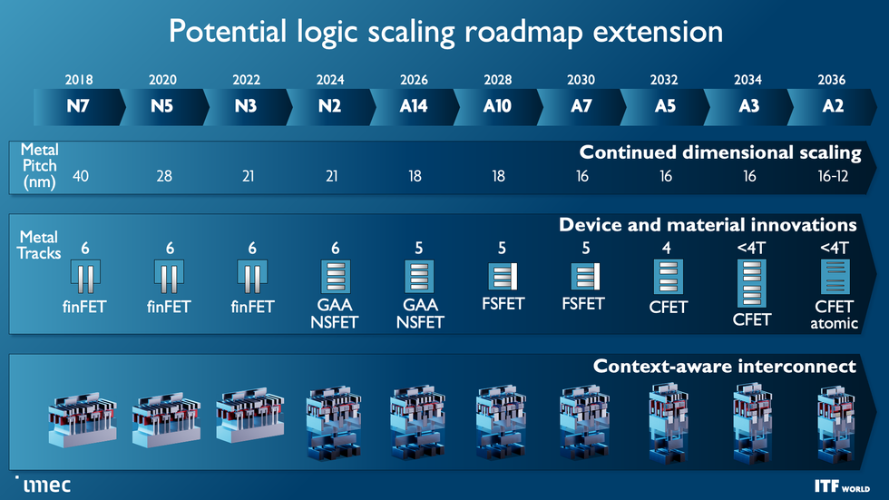
Continued transistor scaling
Main chipmakers are already transitioning from the FinFET transistors that powered the final decade of computer systems and smartphones to a brand new structure, nanosheet transistors [see “The Nanosheet Transistor Is the Next (and Maybe Last) Step in Moore’s Law”]. Finally, two nanosheet transistors will likely be constructed atop one another to type the complementary FET, or CFET, which Velloso says “represents the last word in CMOS scaling” [see “3D-Stacked CMOS Takes Moore’s Law to New Heights”].
As these units scale down and alter form, one of many foremost targets is to drive down the dimensions of ordinary logic cells. That’s sometimes measured in “monitor top”—principally, the variety of steel interconnect strains that may match throughout the cell. Superior FinFETs and early nanosheet units are six-track cells. Transferring to 5 tracks could require an interstitial design referred to as a forksheet, which squeezes units collectively extra intently with out essentially making them smaller. CFETs will then cut back cells to 4 tracks or probably fewer.
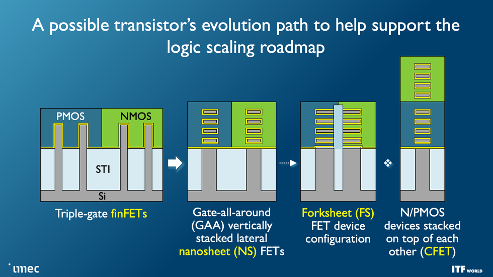 Modern transistors are already transitioning from the fin field-effect transistor (FinFET) structure to nanosheets. The final word purpose is to stack two units atop one another in a CFET configuration. The forksheet could also be an middleman step on the best way.Imec
In line with Imec, chipmakers will be capable to produce the finer options wanted for this development utilizing ASML’s subsequent era of extreme-ultraviolet lithography. That tech, referred to as high-numerical-aperture EUV, is below development at ASML now, and Imec is subsequent in line for supply. Rising numerical aperture, an optics time period associated to the vary of angles over which a system can collect mild, results in extra exact photographs.
Bottom power-delivery networks
The fundamental thought in bottom power-delivery networks is to take away all of the interconnects that ship energy—versus information indicators—from above the silicon floor and place them beneath it. This could permit for much less energy loss, as a result of the facility delivering interconnects might be bigger and fewer resistant. It additionally frees up room above the transistor layer for signal-carrying interconnects, probably resulting in extra compact designs [see “Next-Gen Chips Will Be Powered From Below”].
Sooner or later, much more may very well be moved to the bottom of the silicon. For instance, so-called world interconnects—people who span (comparatively) nice distances to hold clock and different indicators—may go beneath the silicon. Or engineers may add energetic power-delivery units, akin to electrostatic discharge security diodes.
3D integration
There are a number of methods to do 3D integration, however essentially the most superior at present are wafer-to-wafer and die-to-wafer hybrid bonding [see “3 Ways 3D Chip Tech Is Upending Computing”]. These two present the very best density of interconnections between two silicon dies. However this technique requires that the 2 dies are designed collectively, so their features and interconnect factors align, permitting them to behave as a single chip, says Anne Jourdain, principal member of the technical workers. Imec R&D is on monitor to have the ability to produce tens of millions of 3D connections per sq. millimeter within the close to future.
Attending to CMOS 2.0
CMOS 2.0 would take disaggregation and heterogeneous integration to the intense. Relying on which applied sciences make sense for the actual purposes, it may lead to a 3D system that comes with layers of embedded reminiscence, I/O and energy infrastructure, high-density logic, excessive drive-current logic, and large quantities of cache reminiscence.
Attending to that time will take not simply expertise improvement but in addition the instruments and coaching to discern which applied sciences would really enhance a system. As Bardon factors out, smartphones, servers, machine-learning accelerators, and augmented- and virtual-reality methods all have very totally different necessities and constraints. What is smart for one could be a useless finish for the opposite.
From Your Website Articles
Associated Articles Across the Net
