
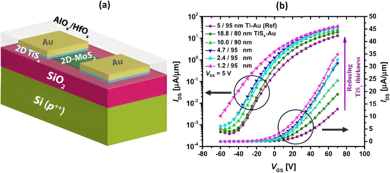
 Schematics of the fabricated MoS2 FETs, (b) measured transfer curves of the devices with series of TiSx contact thicknesses, in both semilog and linear scales. Data for the reference sample is also provided. Credit: Nanoscale Advances (2023). DOI: 10.1039/D3NA00387F")
Two-dimensional transition-metal dichalcogenides (2D TMDs), particularly MoS2, are on the forefront of new-generation 2D supplies, and industrial-level efforts are being made to supply them at a big scale with cheap efficiency for digital gadget purposes. Often, for show purposes, cost provider mobility of two cm2/V.s is ample.
Although mechanically exfoliated MoS2 is well-known to have a lot larger mobility than this, its large-area manufacturing is difficult. Additional, it’s unclear how the efficiency of 2D TMD units shall be if they’re contacted by new technology 2D metals as a substitute of normal 3D metals akin to Au, Ti, Ni, and many others.
Therefore, researchers at Eindhoven College of Expertise (Tue), The Netherlands and SRM Institute of Science and Expertise (SRMIST), India, have reported just lately in Nanoscale Advances on the large-area development of 2D steel TiSx on prime of 2D semiconductor MoS2 by plasma-enhanced atomic layer development (PEALD) method.
It’s totally difficult to optimize the expansion circumstances to acquire an atomically clear interface between such supplies. Researchers discovered that the transistor efficiency of MoS2 is nearly two instances higher when contacted with the 2D steel TiSx in comparison with Ti and Au 3D metals. The pattern was noticed in many of the figures-of-merit of the transistor. This process will be utilized for a lot of such supplies sooner or later.
The cost transport research at numerous temperatures revealed variations within the meta-semiconductor junction barrier top and its affect on contact resistance. To grasp this new system, researchers carried out TCAD gadget simulation to visualise the distribution of cost carriers in atomic layers. It’s observed that within the presence of TiSx, the intrinsic cost provider density of MoS2 will increase, which results in improved efficiency.
These outcomes will enable the metallic contacts in 2D and 3D gadget integration to be thinned down, rising gadget density. This exemplary analysis will play an necessary position in future quantum units and in figuring out new cost transport equations throughout the interface of 2D steel-semiconductors.
Extra data:
Reyhaneh Mahlouji et al, ALD-grown two-dimensional TiSx steel contacts for MoS2 field-effect transistors, Nanoscale Advances (2023). DOI: 10.1039/D3NA00387F
Offered by
SRM Institute of Science and Expertise
Quotation:
Researchers enhance the efficiency of semiconductors utilizing novel 2D steel (2023, August 18)
retrieved 18 August 2023
from https://phys.org/information/2023-08-semiconductors-2nd-metal.html
This doc is topic to copyright. Aside from any honest dealing for the aim of personal research or analysis, no
half could also be reproduced with out the written permission. The content material is offered for data functions solely.
