
Jan 11, 2024
(Nanowerk Highlight) The distinctive properties of natural semiconductors have pushed their growing use in superior electronics and optoelectronics over the previous decade. In comparison with standard inorganic supplies, researchers can customized design the molecules to realize specialised traits. Equally vital is processability at low temperatures and straightforward integration with next-generation gadgets. Nonetheless, a cussed problem has been the lack to manage key progress parameters of nanoscale natural semiconductor buildings that allow sensible purposes.
Particularly, the paper makes use of a way referred to as graphoepitaxy – a mechanism the place nanowires develop alongside the linear orientation outlined by nanoscale floor options on a substrate, relatively than the underlying crystalline construction. This graphoepitaxial steering had already been used to align inorganic nanowires, however preliminary makes an attempt to use it for natural semiconductor buildings like Alq3 yielded randomly scattered growths with no long-range order.
Now, a world group of researchers have reported an modern extension of graphoepitaxy that allows simultaneous management over the alignment course and placement of natural semiconductor nanowires throughout an entire substrate throughout vapor deposition synthesis.
Printed in Superior Practical Supplies (“Selective-Space Progress of Aligned Natural Semiconductor Nanowires and Their Machine Integration”), the approach combines graphoepitaxial steering from nanoscale floor options with microscale shadows from a masks to direct the expansion of extremely ordered natural nanowire arrays in predefined places.
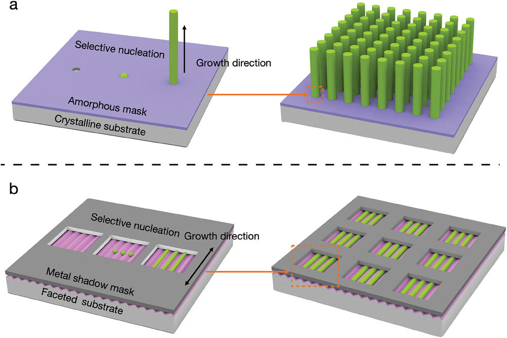 Schematic diagrams of selective-area progress of nanowires in vapor part. a) Earlier selective-area out-of-plane epitaxial progress of aligned nanowires on a flat single-crystalline floor, the place the nanowire positions are decided by nanoscale holes on the coated amorphous masks and the nanowire progress orientation is inherited from the underlying lattice-matched floor. b) Proposed selective-area in-plane graphoepitaxial progress of aligned nanowires on a faceted single-crystalline floor, the place the nanowire positions are decided by micro-sized holes on the coated steel masks and the nanowire progress orientation is outlined by the periodic aspects of the floor. (Reprinted with permission by Wiley-VCH Verlag)
“Having the ability to dictate orientation and site-specificity of natural nanowires in a single progress course of allows their seamless integration into useful gadgets with out damaging handbook manipulation,” explains lead creator Dr. Jinyou Xu.
The brand new progress course of utilized tris(8-hydroxyquinoline)aluminum (Alq3), an natural semiconductor and light-weight emitter. Alq3 nanowires have been synthesized utilizing bodily vapor deposition onto a tailor-made faceted sapphire floor that directed their orientation alongside parallel nanogrooves. This ‘graphoepitaxy’ mechanism had already guided inorganic nanowires however preliminary makes an attempt with Alq3 produced randomly oriented ‘grassy’ growths with no long-range order.
Researchers discovered that modifying the faceted floor with an ultra-thin alkyl coating altered the floor vitality stability and enhanced the interplay between Alq3 molecules throughout deposition. This promoted preferential horizontal alignment alongside the nanogrooves. However nanowire positions have been nonetheless not managed.
To localize growths to particular areas, researchers coated the floor with a shadow masks containing an array of microscale holes, proscribing Alq3 vapor flux to solely straight uncovered areas. Computational fluid simulations revealed that holes induced non-uniform mass transport profiles and boundary layer thickness variations which confined the preliminary nanowire nucleation websites to small areas round gap facilities. Owing to nanoscale geometry, these nucleation websites despatched out unidirectional progress fronts that remained aligned to nanogrooves throughout total holes. This mixed ‘selective-area graphoepitaxy’ approach assembled arrays of extremely oriented Alq3 nanowires with managed densities and lengths based mostly on gap layouts.
Schematic diagrams of selective-area progress of nanowires in vapor part. a) Earlier selective-area out-of-plane epitaxial progress of aligned nanowires on a flat single-crystalline floor, the place the nanowire positions are decided by nanoscale holes on the coated amorphous masks and the nanowire progress orientation is inherited from the underlying lattice-matched floor. b) Proposed selective-area in-plane graphoepitaxial progress of aligned nanowires on a faceted single-crystalline floor, the place the nanowire positions are decided by micro-sized holes on the coated steel masks and the nanowire progress orientation is outlined by the periodic aspects of the floor. (Reprinted with permission by Wiley-VCH Verlag)
“Having the ability to dictate orientation and site-specificity of natural nanowires in a single progress course of allows their seamless integration into useful gadgets with out damaging handbook manipulation,” explains lead creator Dr. Jinyou Xu.
The brand new progress course of utilized tris(8-hydroxyquinoline)aluminum (Alq3), an natural semiconductor and light-weight emitter. Alq3 nanowires have been synthesized utilizing bodily vapor deposition onto a tailor-made faceted sapphire floor that directed their orientation alongside parallel nanogrooves. This ‘graphoepitaxy’ mechanism had already guided inorganic nanowires however preliminary makes an attempt with Alq3 produced randomly oriented ‘grassy’ growths with no long-range order.
Researchers discovered that modifying the faceted floor with an ultra-thin alkyl coating altered the floor vitality stability and enhanced the interplay between Alq3 molecules throughout deposition. This promoted preferential horizontal alignment alongside the nanogrooves. However nanowire positions have been nonetheless not managed.
To localize growths to particular areas, researchers coated the floor with a shadow masks containing an array of microscale holes, proscribing Alq3 vapor flux to solely straight uncovered areas. Computational fluid simulations revealed that holes induced non-uniform mass transport profiles and boundary layer thickness variations which confined the preliminary nanowire nucleation websites to small areas round gap facilities. Owing to nanoscale geometry, these nucleation websites despatched out unidirectional progress fronts that remained aligned to nanogrooves throughout total holes. This mixed ‘selective-area graphoepitaxy’ approach assembled arrays of extremely oriented Alq3 nanowires with managed densities and lengths based mostly on gap layouts.
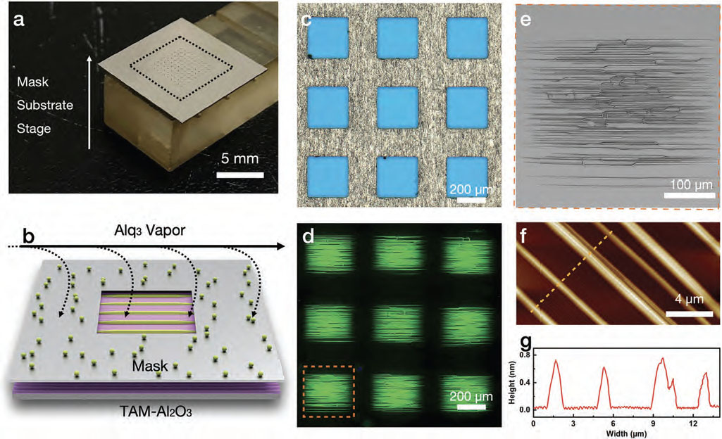 Selective-area progress of self-oriented Alq3 nanowires. a) Digital images and b) schematic diagram of the stacking configuration. The dashed sq. in (a) signifies the substrate place underneath the shadow masks. c) Optical microscopic picture of the steel shadow masks. d) Fluorescence optical microscopic picture of the site-controlled horizontally-aligned Alq3 nanowires underneath UV illumination. e) Consultant SEM picture of the sitecontrolled horizontally-aligned Alq3 nanowires in a micro-sized gap. f) AFM picture and g) peak profile of the Alq3 nanowires. (Reprinted with permission by Wiley-VCH Verlag)
Structural analyses utilizing cross-polarized optical microscopy, electron diffraction and X-ray diffraction verified the single-crystalline nature of Alq3 nanowires with long-range molecular order and preferential progress axis alongside the (01̄1) lattice airplane. An distinctive 75.12% inner quantum effectivity was measured. The aligning mechanism was not contingent on lattice-matching, not like present epitaxial progress methods. Researchers demonstrated micro-scale management to generate oriented Alq3 nanowire arrays with completely different configurations and dimensions throughout a substrate by merely adjusting gap parameters within the shadow masks. Notably, 872 micron lengthy nanowires have been obtained utilizing rectangular holes – a length-to-diameter ratio exceeding 1200.
As-grown nanostructure arrays have been straight built-in into functioning digital gadgets with none nanowire switch or handbook manipulation. A two-terminal gadget exhibited robust unfavourable differential resistance with a 3.97 peak-to-valley present ratio, aggressive with state-of-the-art supplies. This uncommon conductivity profile is enticing for specialised circuit purposes corresponding to recollections, amplifiers and logic switches. Moreover, a definite photoresponse was measured underneath 405 nm illumination with 200 millisecond rise/decay occasions, confirming photosensitivity.
“The proposed selective-area graphoepitaxy technique altered the long-held notion that lattice-matching between crystals is necessary for controlling orientation. Moreover, no steel catalysts have been required,” explains Xu. “The approach opens potentialities of assembling numerous natural molecules into customized oriented nanowire architectures for electronics manufacturing.”
Nonetheless, contact points associated to gadget fabrication want optimized electrode interfaces. Regardless, this breakthrough analysis makes a compelling case that synergistically harnessing self-assembly behaviors on a number of size scales allows scalable bottom-up nanomanufacturing not viable by means of top-down lithography. Importantly, it liberates natural nanowires from constraints of handbook manipulation by directing site-specific orientation-controlled growths.
Selective-area progress of self-oriented Alq3 nanowires. a) Digital images and b) schematic diagram of the stacking configuration. The dashed sq. in (a) signifies the substrate place underneath the shadow masks. c) Optical microscopic picture of the steel shadow masks. d) Fluorescence optical microscopic picture of the site-controlled horizontally-aligned Alq3 nanowires underneath UV illumination. e) Consultant SEM picture of the sitecontrolled horizontally-aligned Alq3 nanowires in a micro-sized gap. f) AFM picture and g) peak profile of the Alq3 nanowires. (Reprinted with permission by Wiley-VCH Verlag)
Structural analyses utilizing cross-polarized optical microscopy, electron diffraction and X-ray diffraction verified the single-crystalline nature of Alq3 nanowires with long-range molecular order and preferential progress axis alongside the (01̄1) lattice airplane. An distinctive 75.12% inner quantum effectivity was measured. The aligning mechanism was not contingent on lattice-matching, not like present epitaxial progress methods. Researchers demonstrated micro-scale management to generate oriented Alq3 nanowire arrays with completely different configurations and dimensions throughout a substrate by merely adjusting gap parameters within the shadow masks. Notably, 872 micron lengthy nanowires have been obtained utilizing rectangular holes – a length-to-diameter ratio exceeding 1200.
As-grown nanostructure arrays have been straight built-in into functioning digital gadgets with none nanowire switch or handbook manipulation. A two-terminal gadget exhibited robust unfavourable differential resistance with a 3.97 peak-to-valley present ratio, aggressive with state-of-the-art supplies. This uncommon conductivity profile is enticing for specialised circuit purposes corresponding to recollections, amplifiers and logic switches. Moreover, a definite photoresponse was measured underneath 405 nm illumination with 200 millisecond rise/decay occasions, confirming photosensitivity.
“The proposed selective-area graphoepitaxy technique altered the long-held notion that lattice-matching between crystals is necessary for controlling orientation. Moreover, no steel catalysts have been required,” explains Xu. “The approach opens potentialities of assembling numerous natural molecules into customized oriented nanowire architectures for electronics manufacturing.”
Nonetheless, contact points associated to gadget fabrication want optimized electrode interfaces. Regardless, this breakthrough analysis makes a compelling case that synergistically harnessing self-assembly behaviors on a number of size scales allows scalable bottom-up nanomanufacturing not viable by means of top-down lithography. Importantly, it liberates natural nanowires from constraints of handbook manipulation by directing site-specific orientation-controlled growths.
Schematic diagrams of selective-area progress of nanowires in vapor part. a) Earlier selective-area out-of-plane epitaxial progress of aligned nanowires on a flat single-crystalline floor, the place the nanowire positions are decided by nanoscale holes on the coated amorphous masks and the nanowire progress orientation is inherited from the underlying lattice-matched floor. b) Proposed selective-area in-plane graphoepitaxial progress of aligned nanowires on a faceted single-crystalline floor, the place the nanowire positions are decided by micro-sized holes on the coated steel masks and the nanowire progress orientation is outlined by the periodic aspects of the floor. (Reprinted with permission by Wiley-VCH Verlag)
“Having the ability to dictate orientation and site-specificity of natural nanowires in a single progress course of allows their seamless integration into useful gadgets with out damaging handbook manipulation,” explains lead creator Dr. Jinyou Xu.
The brand new progress course of utilized tris(8-hydroxyquinoline)aluminum (Alq3), an natural semiconductor and light-weight emitter. Alq3 nanowires have been synthesized utilizing bodily vapor deposition onto a tailor-made faceted sapphire floor that directed their orientation alongside parallel nanogrooves. This ‘graphoepitaxy’ mechanism had already guided inorganic nanowires however preliminary makes an attempt with Alq3 produced randomly oriented ‘grassy’ growths with no long-range order.
Researchers discovered that modifying the faceted floor with an ultra-thin alkyl coating altered the floor vitality stability and enhanced the interplay between Alq3 molecules throughout deposition. This promoted preferential horizontal alignment alongside the nanogrooves. However nanowire positions have been nonetheless not managed.
To localize growths to particular areas, researchers coated the floor with a shadow masks containing an array of microscale holes, proscribing Alq3 vapor flux to solely straight uncovered areas. Computational fluid simulations revealed that holes induced non-uniform mass transport profiles and boundary layer thickness variations which confined the preliminary nanowire nucleation websites to small areas round gap facilities. Owing to nanoscale geometry, these nucleation websites despatched out unidirectional progress fronts that remained aligned to nanogrooves throughout total holes. This mixed ‘selective-area graphoepitaxy’ approach assembled arrays of extremely oriented Alq3 nanowires with managed densities and lengths based mostly on gap layouts.
Selective-area progress of self-oriented Alq3 nanowires. a) Digital images and b) schematic diagram of the stacking configuration. The dashed sq. in (a) signifies the substrate place underneath the shadow masks. c) Optical microscopic picture of the steel shadow masks. d) Fluorescence optical microscopic picture of the site-controlled horizontally-aligned Alq3 nanowires underneath UV illumination. e) Consultant SEM picture of the sitecontrolled horizontally-aligned Alq3 nanowires in a micro-sized gap. f) AFM picture and g) peak profile of the Alq3 nanowires. (Reprinted with permission by Wiley-VCH Verlag)
Structural analyses utilizing cross-polarized optical microscopy, electron diffraction and X-ray diffraction verified the single-crystalline nature of Alq3 nanowires with long-range molecular order and preferential progress axis alongside the (01̄1) lattice airplane. An distinctive 75.12% inner quantum effectivity was measured. The aligning mechanism was not contingent on lattice-matching, not like present epitaxial progress methods. Researchers demonstrated micro-scale management to generate oriented Alq3 nanowire arrays with completely different configurations and dimensions throughout a substrate by merely adjusting gap parameters within the shadow masks. Notably, 872 micron lengthy nanowires have been obtained utilizing rectangular holes – a length-to-diameter ratio exceeding 1200.
As-grown nanostructure arrays have been straight built-in into functioning digital gadgets with none nanowire switch or handbook manipulation. A two-terminal gadget exhibited robust unfavourable differential resistance with a 3.97 peak-to-valley present ratio, aggressive with state-of-the-art supplies. This uncommon conductivity profile is enticing for specialised circuit purposes corresponding to recollections, amplifiers and logic switches. Moreover, a definite photoresponse was measured underneath 405 nm illumination with 200 millisecond rise/decay occasions, confirming photosensitivity.
“The proposed selective-area graphoepitaxy technique altered the long-held notion that lattice-matching between crystals is necessary for controlling orientation. Moreover, no steel catalysts have been required,” explains Xu. “The approach opens potentialities of assembling numerous natural molecules into customized oriented nanowire architectures for electronics manufacturing.”
Nonetheless, contact points associated to gadget fabrication want optimized electrode interfaces. Regardless, this breakthrough analysis makes a compelling case that synergistically harnessing self-assembly behaviors on a number of size scales allows scalable bottom-up nanomanufacturing not viable by means of top-down lithography. Importantly, it liberates natural nanowires from constraints of handbook manipulation by directing site-specific orientation-controlled growths.

By
Michael
Berger
– Michael is creator of three books by the Royal Society of Chemistry:
Nano-Society: Pushing the Boundaries of Expertise,
Nanotechnology: The Future is Tiny, and
Nanoengineering: The Abilities and Instruments Making Expertise Invisible
Copyright ©
Nanowerk LLC
Develop into a Highlight visitor creator! Be a part of our giant and rising group of visitor contributors. Have you ever simply printed a scientific paper or produce other thrilling developments to share with the nanotechnology group? Right here is the way to publish on nanowerk.com.
