

In a brand new examine revealed in ACS Nano, researchers from the Harvard John A. Paulson Faculty of Engineering and Utilized Sciences (SEAS) have unveiled a 10-centimeter-diameter glass metalens able to taking high-resolution pictures of celestial our bodies just like the solar, moon, and distant nebulae.
This breakthrough, marking the primary large-scale, visible-wavelength metalens crafted fully from glass, could be mass-produced with conventional CMOS manufacturing methods.
The power to precisely management the scale of tens of billions of nanopillars over an unprecedentedly massive flat lens utilizing state-of-the-art semiconductor foundry processes is a nanofabrication feat that opens thrilling new alternatives for area science and expertise.
Federico Capasso, Research Senior Creator and Robert L. Wallace Professor of Utilized Physics, Harvard John A. Paulson Faculty of Engineering and Utilized Sciences (SEAS), Harvard College
Most flat metalenses are across the measurement of a chunk of glitter and focus mild utilizing thousands and thousands of pillar-like nanostructures. Through the use of a way often called deep-ultraviolet (DUV) projection lithography, Capasso and his colleagues created a centimeter-scale metalens in 2019.
This methodology eliminates the laborious writing and deposition processes vital for earlier metalenses and tasks a nanostructure sample that may be straight etched into the glass wafer.
Effective strains and shapes are sometimes patterned in silicon chips for computer systems and cellphones utilizing DUV projection lithography. As a present postdoctoral fellow in Capasso’s lab and a graduate pupil at SEAS, Joon-Suh Park confirmed that the expertise may produce the metalenses at scale and enlarge them for utilization in digital and augmented actuality functions.
Nonetheless, there was an engineering problem to make the metalens considerably bigger for astronomy and free-space optical communications functions.
There’s a main limitation with the lithography instrument as a result of these instruments are used to make laptop chips, so chip measurement is restricted to not more than 20 to 30 millimeters. To be able to make a 100-millimeter diameter lens, we would have liked to discover a manner round this limitation.
Joon-Suh Park, Postdoctoral Fellow, Harvard John A. Paulson Faculty of Engineering and Utilized Sciences (SEAS), Harvard College
Park and colleagues created a way for using the DUV projection lithography instrument to piece collectively a number of nanopillar designs. In just some minutes, the researchers demonstrated that DUV projection lithography may sample 18.7 billion deliberate nanostructures onto a 10-centimeter round area by splitting the lens into twenty-five elements and solely utilizing the 7 sections of a quadrant that took rotational symmetry under consideration.
The group additionally created a vertical glass etching methodology that allows the etching of clean sidewall and excessive side ratio nanopillars into glass.
Utilizing the identical DUV projection lithography, one may produce large-diameter, aberration-correcting meta-optics and even bigger lenses on bigger glass diameter wafers because the corresponding CMOS foundry instruments change into more and more out there within the business.
Quickly Wei Daniel Lim, Research Co-First Creator and Postdoctoral Fellow, Harvard John A. Paulson Faculty of Engineering and Utilized Sciences (SEAS), Harvard College
Lim was the primary contributor to the excellent simulation and characterization of all potential fabrication faults that may happen throughout mass-manufacturing procedures and the way they may have an effect on metalenses’ optical efficiency.
The researchers then addressed potential manufacturing points earlier than showcasing the metalens’ capability to picture astronomical objects.
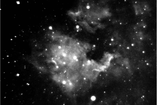
Park and the group went to the roof of Harvard’s Science Middle and mounted the metalens on a tripod geared up with a colour filter and a digital camera sensor. There, they captured pictures of the Solar, Moon, and North America Nebula, a faint nebula positioned 2,590 light-years away within the constellation Cygnus.
Arman Amirzhan, a graduate pupil within the Capasso Lab and co-author of the examine, added, “We have been capable of get very detailed pictures of the Solar, the moon and the nebula which are comparable to photographs taken by standard lenses.”
The researchers have been capable of seize the identical sunspot cluster as a NASA picture from that very same day, utilizing solely the metalens.
The group additionally confirmed that the lens wouldn’t endure any injury or lack of optical operate from publicity to extraordinarily excessive or low temperatures in addition to the sturdy vibrations that might be skilled throughout an area launch.
The lens may probably be utilized for directed power transmission and long-distance telecommunications resulting from its measurement and monolithic glass composition.
Hyukmo Kang, Karlene Karrfalt, Daewook Kim, Joel Leger, Augustine Urbas, Marcus Ossiander, and Zhaoyi Li are co-authors of the examine. It was funded by the Air Drive Workplace of Scientific Analysis below Award No. FA9550-22-1-0312 and the Protection Superior Analysis Tasks Company (DARPA) below Grant No. HR00111810001.
Journal Reference:
Park, J.-S., et. al. (2023) All-Glass 100 mm Diameter Seen Metalens for Imaging the Cosmos. ACS Nano. doi:10.1021/acsnano.3c09462.
Supply: https://seas.harvard.edu/
