
(Nanowerk Information) Creating novel supplies by combining layers with distinctive, helpful properties looks as if a reasonably intuitive course of—stack up the supplies and stack up the advantages. This isn’t at all times the case, nevertheless. Not each materials will permit power to journey by means of it the identical method, making the advantages of 1 materials come at the price of one other. Utilizing cutting-edge instruments, scientists on the Heart for Purposeful Nanomaterials (CFN), a U.S. Division of Vitality (DOE) Consumer Facility at Brookhaven Nationwide Laboratory, and the Institute of Experimental Physics on the College of Warsaw have created a brand new layered construction with 2D materials that reveals a singular switch of power and cost. Understanding its materials properties might result in developments in applied sciences like photo voltaic cells and different optoelectronic gadgets. The outcomes have been printed in Nano Letters (“Excitation-Dependent Excessive-Mendacity Excitonic Trade through Interlayer Vitality Switch from Decrease-to-Greater Bandgap 2D Materials”).
2D Supplies – Tiny, however Mighty
Transition steel dichalcogenides (TMDs) are a category of supplies structured like sandwiches with atomically skinny layers. The meat of a TMD is a transition steel, which may kind chemical bonds with electrons on their outermost orbit or shell, like most components, in addition to the subsequent shell. That steel is sandwiched between two layers of chalcogens, a class of components that comprises oxygen, sulfur, and selenium. Chalcogens all have six electrons of their outermost shell, which makes their chemical habits related. Every of those materials layers is just one atom thick—one-millionth the thickness of a strand of human hair—main them to be known as two-dimensional (2D) supplies. “On the atomic stage, you get to see these distinctive and tunable digital properties,” mentioned Abdullah Al-Mahboob, a Brookhaven workers scientist within the CFN Interface Science and Catalysis group. “TMDs are like a playground of physics. We’re transferring power round from one materials to the opposite at an atomic stage.” Some new properties begin to emerge from supplies at this scale. Graphene, for instance, is the 2D model of graphite, the fabric that the majority pencils are made from. In a Nobel Prize-winning experiment, scientists used a bit of adhesive tape to tug flakes off of graphite to review a layer of graphene. The researchers discovered the graphene to be extremely robust on the atomic stage—200 occasions stronger than metal relative to its weight! As well as, graphene is a superb thermal and electrical conductor and has a singular mild absorption spectrum. This unlocked the door to learning the 2D types of different supplies and their properties. 2D supplies are attention-grabbing on their very own, however when mixed, shocking issues begin to occur. Every materials has its personal superpower—defending supplies from the setting, controlling the switch of power, absorbing mild in several frequencies—and when scientists begin to stack them collectively, they create what is called a heterostructure. These heterostructures are able to some extraordinary issues and will sooner or later be built-in into future applied sciences, like smaller digital elements and extra superior mild detectors.QPress—A First-of-its-Form Experimental Instrument
Whereas the exploration of those supplies might have began with one thing so simple as a bit of adhesive tape, the instruments used to extract, isolate, catalog, and construct 2D supplies have turn into fairly superior. At CFN, a complete system has been devoted to the research of those heterostructures and the methods used to create them—the Quantum Materials Press (QPress). The QPress facility at CFN. (Picture: Brookhaven Nationwide Laboratory)
“It’s exhausting to check the QPress to something,” mentioned Suji Park, a Brookhaven workers scientist specializing in digital supplies. “It builds a construction layer by layer, like a 3D printer, however 2D heterostructures are constructed by a completely completely different strategy. The QPress creates materials layers which might be an atom or two thick, analyzes them, catalogs them, and at last assembles them. Robotics is used to systematically fabricate these ultrathin layers to create novel heterostructures.”
The QPress has three customized constructed modules—the exfoliator, cataloger, and stacker. To create 2D layers, scientists use the exfoliator. Much like the handbook adhesive tape method, the exfoliator has a mechanized curler meeting that exfoliates skinny layers from bigger supply crystals with controls that present the sort of precision that may’t be achieved by hand. As soon as collected and distributed, the supply crystals are pressed onto a silicone oxide wafer and peeled off. They’re then handed alongside to the cataloger, an automatic microscope combing a number of optical characterization methods. The cataloger makes use of machine studying (ML) to determine flakes of curiosity which might be then cataloged right into a database. Presently, ML is educated with solely graphene knowledge, however researchers will hold including completely different sorts of 2D supplies. Scientists can use this database to search out the fabric flakes they want for his or her analysis.
When the required supplies can be found, scientists can use the stacker to manufacture heterostructures from them. Utilizing high-precision robotics, they take the pattern flakes and organize them within the order wanted, at any needed angle, and switch substrates to create the ultimate heterostructure, which will be saved long-term in a pattern library for later use. The local weather is managed to make sure the standard of the samples and the fabrication course of from exfoliation to constructing heterostructures is carried out in an inert fuel setting in a glovebox. The exfoliated flakes and the stacked samples are saved in vacuum, within the pattern libraries of the QPress cluster. Moreover, electron beam evaporation, annealing, and oxygen plasma instruments can be found within the vacuum facet of the cluster. Robotics are used to go samples from one space of the QPress to the subsequent. As soon as these novel heterostructures are fabricated although, what do they really do and the way do they do it?
After the group at CFN fabricated these fascinating new supplies with the QPress, they built-in the supplies with a collection of superior microscopy and spectroscopy instruments that enabled them to discover optoelectronic properties with out exposing the samples to air, which might degrade materials constructions. Among the delicate, unique quantum properties on 2D supplies want ultra-low cryo-temperatures to be detected, all the way down to only a few kelvins. In any other case, they get perturbed by the slightest quantity of warmth or any chemical substances current within the air.
Al-Mahboob’s work is funded by the DOE Quantum Supplies: Built-in Multimodal Characterization and Processing (QM-IMCP) challenge that CFN has began to construct. This platform will embody superior microscopes, x-ray spectrometers, and ultrafast lasers which might be capable of examine the quantum world at cryo-temperatures.
The QPress facility at CFN. (Picture: Brookhaven Nationwide Laboratory)
“It’s exhausting to check the QPress to something,” mentioned Suji Park, a Brookhaven workers scientist specializing in digital supplies. “It builds a construction layer by layer, like a 3D printer, however 2D heterostructures are constructed by a completely completely different strategy. The QPress creates materials layers which might be an atom or two thick, analyzes them, catalogs them, and at last assembles them. Robotics is used to systematically fabricate these ultrathin layers to create novel heterostructures.”
The QPress has three customized constructed modules—the exfoliator, cataloger, and stacker. To create 2D layers, scientists use the exfoliator. Much like the handbook adhesive tape method, the exfoliator has a mechanized curler meeting that exfoliates skinny layers from bigger supply crystals with controls that present the sort of precision that may’t be achieved by hand. As soon as collected and distributed, the supply crystals are pressed onto a silicone oxide wafer and peeled off. They’re then handed alongside to the cataloger, an automatic microscope combing a number of optical characterization methods. The cataloger makes use of machine studying (ML) to determine flakes of curiosity which might be then cataloged right into a database. Presently, ML is educated with solely graphene knowledge, however researchers will hold including completely different sorts of 2D supplies. Scientists can use this database to search out the fabric flakes they want for his or her analysis.
When the required supplies can be found, scientists can use the stacker to manufacture heterostructures from them. Utilizing high-precision robotics, they take the pattern flakes and organize them within the order wanted, at any needed angle, and switch substrates to create the ultimate heterostructure, which will be saved long-term in a pattern library for later use. The local weather is managed to make sure the standard of the samples and the fabrication course of from exfoliation to constructing heterostructures is carried out in an inert fuel setting in a glovebox. The exfoliated flakes and the stacked samples are saved in vacuum, within the pattern libraries of the QPress cluster. Moreover, electron beam evaporation, annealing, and oxygen plasma instruments can be found within the vacuum facet of the cluster. Robotics are used to go samples from one space of the QPress to the subsequent. As soon as these novel heterostructures are fabricated although, what do they really do and the way do they do it?
After the group at CFN fabricated these fascinating new supplies with the QPress, they built-in the supplies with a collection of superior microscopy and spectroscopy instruments that enabled them to discover optoelectronic properties with out exposing the samples to air, which might degrade materials constructions. Among the delicate, unique quantum properties on 2D supplies want ultra-low cryo-temperatures to be detected, all the way down to only a few kelvins. In any other case, they get perturbed by the slightest quantity of warmth or any chemical substances current within the air.
Al-Mahboob’s work is funded by the DOE Quantum Supplies: Built-in Multimodal Characterization and Processing (QM-IMCP) challenge that CFN has began to construct. This platform will embody superior microscopes, x-ray spectrometers, and ultrafast lasers which might be capable of examine the quantum world at cryo-temperatures.
Constructing Higher Constructions
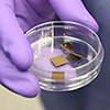
Utilizing the superior capabilities of those assets, the group was capable of get a extra detailed image of how long-distance power switch works in TMDs.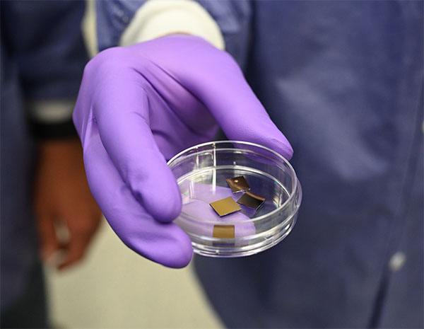 Samples of the transition steel dichalcogenides. (Picture: Brookhaven Nationwide Laboratory)
Vitality needs to maneuver throughout supplies, the way in which an individual needs to climb a ladder, however it wants a spot to carry on to. Bandgaps will be considered the area between the rungs of a ladder. The bigger the hole, the tougher and slower it’s to climb. If the hole is simply too giant, it won’t even be potential to complete transferring up. Utilizing supplies that have already got nice conducting properties, this specialised group of scientists was capable of stack them in a method that leveraged their construction to create pathways that switch the cost extra effectively.
One of many TMDs the group created was molybdenum disulfide (MoS2), which was proven in earlier research to have robust photoluminescence. Photoluminescence is the phenomenon that makes sure supplies glow at the hours of darkness after they’re uncovered to mild. When a cloth absorbs mild with extra power than that power bandgap, it may emit mild with photon power equal to the bandgap power. If a second materials with an equal or decrease power bandgap will get nearer to the primary, as shut as a sub-nanometer to few nanometers, power can switch nonradiatively from the primary materials to the second. The second materials can then emit mild with photon power equal to its power bandgap.
With an insulating interlayer made from hexagonal boron nitride (hBN), which prevents digital conductivity, scientists noticed an uncommon sort of long-distance power switch between this TMD and one made from tungsten diselenide (WSe2), which conducts electrical energy very effectively. The power switch course of occurred from the lower-to-higher bandgap supplies, which isn’t typical in TMD heterostructures, the place the switch normally happens from the higher-to-lower bandgap 2D supplies. The thickness of the interlayer performed an enormous function, but additionally appeared to defy expectations.
“We have been shocked by the habits of this materials,” mentioned Al-Mahboob. “The interplay between the 2 layers will increase together with the rise in distance as much as a sure diploma, after which it begins to lower. Variables like spacing, temperature, and angle performed an vital function.”
By gaining a greater understanding of how these supplies take in and emit power at this scale, scientists can apply these properties to new kinds of applied sciences and enhance present ones. These may embody photo voltaic cells that take in mild extra successfully and maintain a greater cost, photosensors with larger accuracy, and digital elements that may be scaled all the way down to even smaller sizes for extra compact gadgets.
Samples of the transition steel dichalcogenides. (Picture: Brookhaven Nationwide Laboratory)
Vitality needs to maneuver throughout supplies, the way in which an individual needs to climb a ladder, however it wants a spot to carry on to. Bandgaps will be considered the area between the rungs of a ladder. The bigger the hole, the tougher and slower it’s to climb. If the hole is simply too giant, it won’t even be potential to complete transferring up. Utilizing supplies that have already got nice conducting properties, this specialised group of scientists was capable of stack them in a method that leveraged their construction to create pathways that switch the cost extra effectively.
One of many TMDs the group created was molybdenum disulfide (MoS2), which was proven in earlier research to have robust photoluminescence. Photoluminescence is the phenomenon that makes sure supplies glow at the hours of darkness after they’re uncovered to mild. When a cloth absorbs mild with extra power than that power bandgap, it may emit mild with photon power equal to the bandgap power. If a second materials with an equal or decrease power bandgap will get nearer to the primary, as shut as a sub-nanometer to few nanometers, power can switch nonradiatively from the primary materials to the second. The second materials can then emit mild with photon power equal to its power bandgap.
With an insulating interlayer made from hexagonal boron nitride (hBN), which prevents digital conductivity, scientists noticed an uncommon sort of long-distance power switch between this TMD and one made from tungsten diselenide (WSe2), which conducts electrical energy very effectively. The power switch course of occurred from the lower-to-higher bandgap supplies, which isn’t typical in TMD heterostructures, the place the switch normally happens from the higher-to-lower bandgap 2D supplies. The thickness of the interlayer performed an enormous function, but additionally appeared to defy expectations.
“We have been shocked by the habits of this materials,” mentioned Al-Mahboob. “The interplay between the 2 layers will increase together with the rise in distance as much as a sure diploma, after which it begins to lower. Variables like spacing, temperature, and angle performed an vital function.”
By gaining a greater understanding of how these supplies take in and emit power at this scale, scientists can apply these properties to new kinds of applied sciences and enhance present ones. These may embody photo voltaic cells that take in mild extra successfully and maintain a greater cost, photosensors with larger accuracy, and digital elements that may be scaled all the way down to even smaller sizes for extra compact gadgets.
