Jan 12, 2024
(Nanowerk Information) Moore’s Legislation, a basic scaling precept for digital units, forecasts that the variety of transistors on a chip will double each two years, making certain extra computing energy — however a restrict exists.
Immediately’s most superior chips home almost 50 billion transistors inside an area no bigger than your thumbnail. The duty of cramming much more transistors into that confined space has grow to be an increasing number of troublesome, in keeping with Penn State researchers.
In a research revealed within the journal Nature (“Three-dimensional integration of two-dimensional field-effect transistors”), Saptarshi Das, an affiliate professor of engineering science and mechanics and co-corresponding creator of the research, and his crew recommend a treatment: seamlessly implementing 3D integration with 2D supplies.
Key Takeaways
Moore’s Legislation, predicting the doubling of transistors on a chip each two years, faces limitations resulting from house constraints on present chips.
A novel strategy involving 3D integration with 2D supplies is proposed to beat these constraints, enabling extra transistors and functionalities.
Monolithic 3D integration, a technique of fabricating semiconductor units, guarantees increased density and house effectivity with out the necessity for microbumps utilized in conventional strategies.
The brand new methodology considerably reduces the method temperature, preserving the integrity of silicon-based chips and making it appropriate with 2D supplies.
This development in semiconductor know-how not solely aligns with Moore’s Legislation but additionally introduces extra functionalities, doubtlessly remodeling the electronics trade.
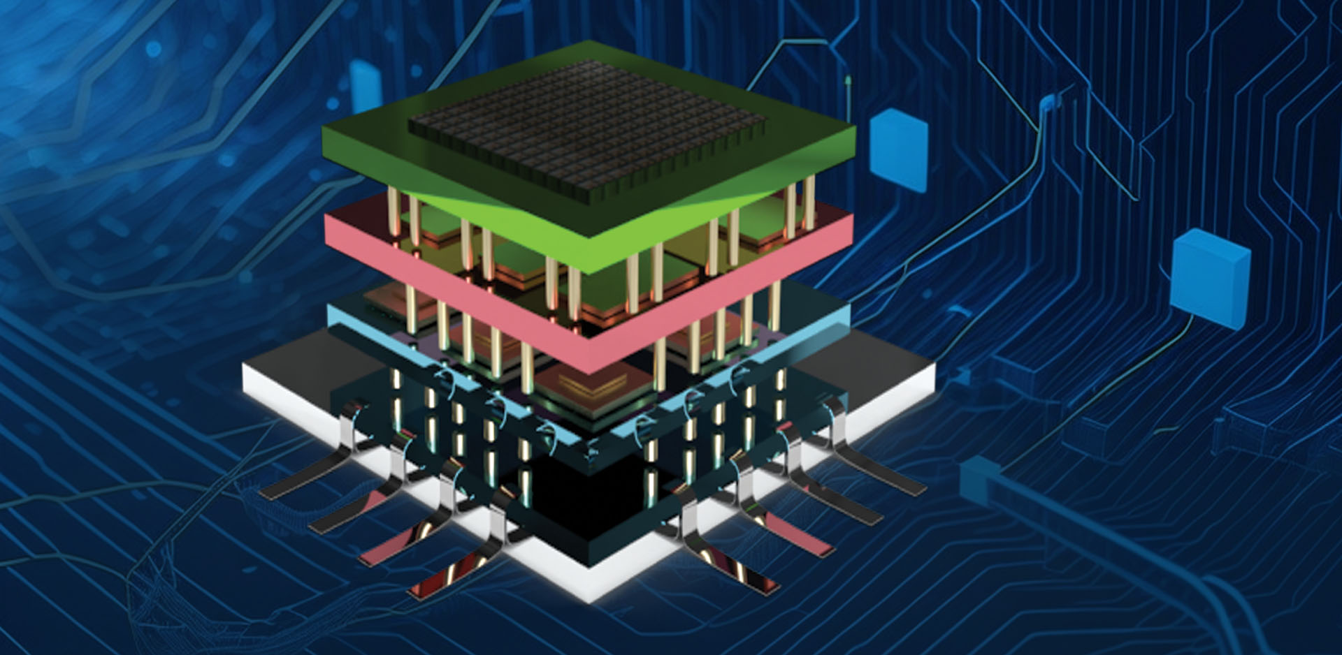
Penn State researchers demonstrated 3D integration of semiconductors at a large scale, characterizing tens of 1000’s of units utilizing 2D transistors made with 2D semiconductors, enabling digital devices to presumably grow to be smarter and extra versatile. (Picture: Elizabeth Flores-Gomez Murray, Supplies Analysis Institute)
The Analysis
Within the semiconductor world, 3D integration means vertically stacking a number of layers of semiconductor units. This strategy not solely facilitates the packing of extra silicon-based transistors onto a pc chip, generally known as “Extra Moore,” but additionally permits the usage of transistors created from 2D supplies to include numerous functionalities inside varied layers of the stack, an idea often known as “Greater than Moore.”
With the work outlined within the research, Saptarshi and the crew show possible paths past scaling present tech to attain each Extra Moore and Greater than Moore via monolithic 3D integration. Monolithic 3D integration is a fabrication course of whereby researchers instantly make the units on the one beneath, as in comparison with the standard means of stacking independently fabricated layers.
“Monolithic 3D integration gives the very best density of vertical connections because it doesn’t depend on bonding of two pre-patterned chips — which might require microbumps the place two chips are bonded collectively — so you might have extra space to make connections,” stated Najam Sakib, graduate analysis assistant in engineering science and mechanics and co-author of the research.
Monolithic 3D integration faces vital challenges, although, in keeping with Darsith Jayachandran, graduate analysis assistant in engineering science and mechanics and co-corresponding creator of the research, since typical silicon parts would soften beneath the processing temperatures.
“One problem is the method temperature ceiling of 450 levels Celsius (C) for back-end integration for silicon-based chips — our monolithic 3D integration strategy drops that temperate considerably to lower than 200 C,” Jayachandran stated, explaining that the method temperature ceiling is the utmost temperature allowed earlier than damaging the prefabricated buildings. “Incompatible course of temperature budgets make monolithic 3D integration difficult with silicon chips, however
2D supplies can stand up to temperatures wanted for the method.”
The researchers used present methods for his or her strategy, however they’re the primary to efficiently obtain monolithic 3D integration at this scale utilizing 2D transistors made with 2D semiconductors referred to as
transition metallic dichalcogenides.
The power to vertically stack the units in 3D integration additionally enabled extra energy-efficient computing as a result of it solved a shocking drawback for such tiny issues as transistors on a pc chip: distance.
“By stacking units vertically on high of one another, you are reducing the gap between units, and due to this fact, you are reducing the lag and in addition the facility consumption,” stated Rahul Pendurthi, graduate analysis assistant in engineering science and mechanics and co-corresponding creator of the research.
By reducing the gap between units, the researchers achieved “Extra Moore.” By incorporating transistors made with 2D supplies, the researchers met the “Greater than Moore” criterion as effectively. The 2D supplies are identified for his or her distinctive digital and optical properties, together with sensitivity to gentle, which makes these supplies ultimate as sensors. That is helpful, the researchers stated, because the variety of related units and edge units — issues like smartphones or wi-fi residence climate stations that collect knowledge on the ‘edge’ of a community — proceed to extend.
“’Extra Than Moore’ refers to an idea within the tech world the place we’re not simply making laptop chips smaller and quicker, but additionally with extra functionalities,” stated Muhtasim Ul Karim Sadaf, graduate analysis assistant in engineering science and mechanics and co-author of the research. “It’s about including new and helpful options to our digital units, like higher sensors, improved battery administration or different particular capabilities, to make our devices smarter and extra versatile.”
Utilizing 2D units for 3D integration has a number of different benefits, the researchers stated. One is superior provider mobility, which refers to how {an electrical} cost is carried in semiconductor supplies. One other is being ultra-thin, enabling the researchers to suit extra transistors on every tier of the 3D integration and allow extra computing energy.
Whereas most educational analysis includes small-scale prototypes, this research demonstrated 3D integration at a large scale, characterizing tens of 1000’s of units. In accordance with Das, this achievement bridges the hole between academia and trade and will result in future partnerships the place trade leverages Penn State’s 2D supplies experience and amenities. The advance in scaling was enabled by the supply of high-quality, wafer-scale transition metallic dichalcogenides developed by researchers at Penn State’s Two-Dimensional Crystal Consortium (2DCC-MIP), a U.S. Nationwide Science Basis (NSF) Supplies Innovation Platform and nationwide person facility.
“This breakthrough demonstrates but once more the important function of supplies analysis as the muse of the semiconductor trade and U.S. competitiveness,” stated Charles Ying, program director for NSF’s Supplies Innovation Platforms. “Years of effort by Penn State’s Two-Dimensional Crystal Consortium to enhance the standard and dimension of 2D supplies have made it attainable to attain 3D integration of semiconductors at a dimension that may be transformative for electronics.”
In accordance with Das, this technological development is simply step one.
“Our capacity to show, at wafer scale, an enormous variety of units exhibits that now we have been in a position to translate this analysis to a scale which may be appreciated by the semiconductor trade,” Das stated. “We’ve got put 30,000 transistors in every tier, which can be a document quantity. This places Penn State in a really distinctive place to guide a few of the work and companion with the U.S. semiconductor trade in advancing this analysis.”

