
Because the world turns into extra technology-driven than ever, there may be an rising demand for higher and faster electronics and computer systems. Spintronics is a brand new innovation that encodes information utilizing an electron’s spin in addition to its cost state, thereby making the entire system quicker and extra environment friendly.
Picture Credit score: Tokyo Institute of Expertise.
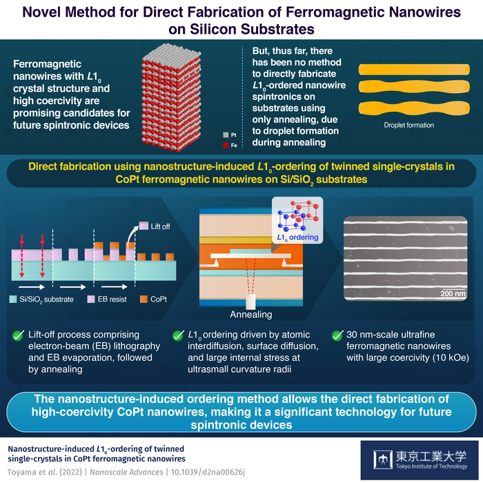
To appreciate the potential of spintronics, ferromagnetic nanowires with robust coercivity (resistance to adjustments in magnetization) are required, and L10-ordered (a type of crystal construction) cobalt–platinum (CoPt) nanowires particularly.
Conventional fabrication processes for L10-ordered nanowires embody warmth therapy to boost the bodily and chemical properties of the fabric, annealing on the crystal substrate; sample switch onto the substrate by way of lithography; and ultimately, chemical layer elimination by way of etching.
Eradicating the etching process by instantly manufacturing nanowires onto the silicon substrate may lead to a major breakthrough in spintronic machine fabrication. Sadly, when instantly fabricated nanowires are annealed, the inherent stresses within the wire trigger them to vary into droplets.
A bunch of scientists headed by Professor Yutaka Majima of the Tokyo Institute of Expertise has found an answer to the issue. The researchers described a brand new fabrication methodology for producing L10-ordered CoPt nanowires on silicon/silicon dioxide (Si/SiO2) substrates. The examine was printed within the journal Nanoscale Advances.
Our nanostructure-induced ordering methodology permits the direct fabrication of ultrafine L10-ordered CoPt nanowires with the slim widths of 30nm scale required for spintronics. This fabrication methodology may additional be utilized to different L10-ordered ferromagnetic supplies reminiscent of iron–platinum and iron–palladium compounds.
Yutaka Majima, Professor, Tokyo Institute of Expertise
On this work, the investigators first coated a Si/SiO2 substrate with a substance known as a “resist” and uncovered it to electron beam lithography and evaporation to kind a stencil for the nanowires.
The substrate was then lined with a multilayer of CoPt. The deposited samples have been then “lifted off,” leaving CoPt nanowires behind, and the nanowires have been then annealed at excessive temperatures. The group additionally used numerous characterization methods to guage the produced nanowires.
Researchers found that the nanowires acquired L10-ordering all through the annealing process. This transition was brought on by atomic interdiffusion, floor diffusion, and exceptionally excessive inside stress on the nanowires’ ultrasmall curvature radii of 10 nm. In addition they found that the nanowires have a excessive coercivity of 10 kiloOersteds (kOe).
The inner stresses on the nanostructure right here induce the L10-ordering. This can be a completely different mechanism than in earlier research. We’re hopeful that this discovery will open up a brand new subject of analysis known as ‘nanostructure-induced supplies science and engineering.’
Yutaka Majima, Professor, Tokyo Institute of Expertise
The breakthrough fabrication approach’s broad applicability and ease of use will undoubtedly make a considerable contribution to the sphere of spintronics analysis.
Journal Reference
Toyama, R., et al. (2022) Nanostructure-induced L10-ordering of twinned single-crystals in CoPt ferromagnetic nanowires. Nanoscale Advances. doi.org/10.1039/D2NA00626J.
Supply: https://www.titech.ac.jp/english
