
(Nanowerk Information) A research displaying how electrons move round sharp bends, comparable to these present in built-in circuits, has the potential to enhance how these circuits, generally utilized in digital and optoelectronic units, are designed.
It has been identified theoretically for about 80 years that when electrons journey round bends, they have a tendency to warmth up as a result of their move strains get squished regionally. Till now, nonetheless, nobody had measured the warmth, for which imaging the move strains is first wanted.
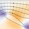
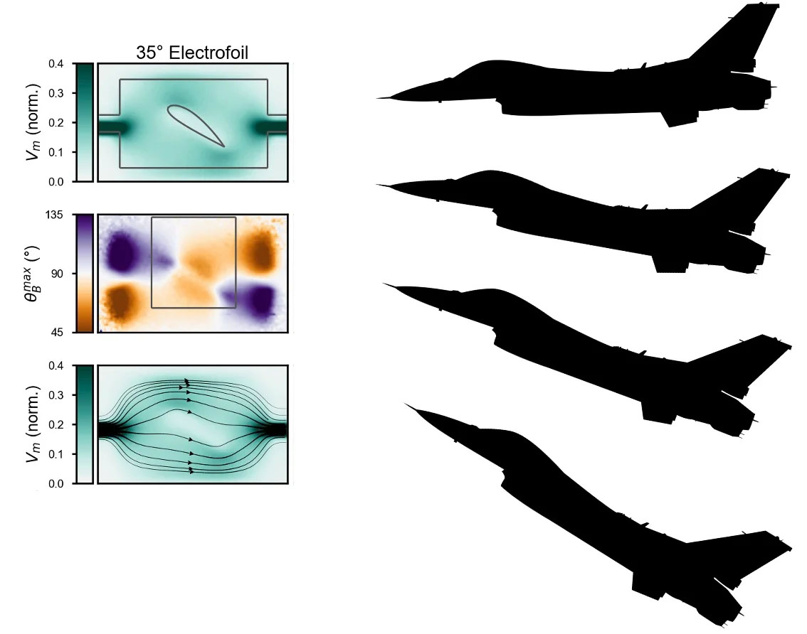
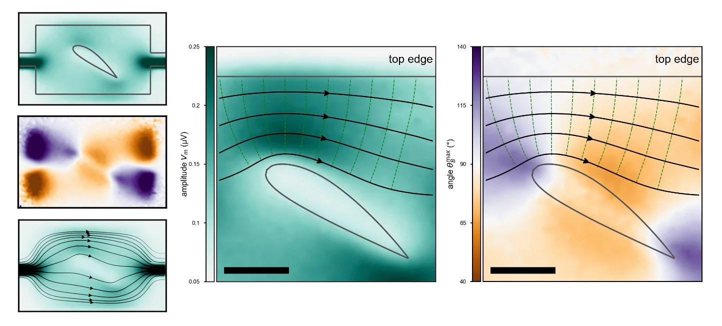 The researchers engineered micromagnetic wing formed units, referred to as electrofoils, which allowed them to exactly contort, compress, and decompress flowlines of digital cost. (Picture: UCR, QMO Lab)
The analysis workforce, led by Nathaniel M. Gabor on the College of California, Riverside, imaged streamlines of electrical present by designing an “electrofoil,” a brand new sort of system that permits for the contortion, compression, and enlargement of streamlines of electrical currents in the identical means airplane wings contort, compress, and develop the move of air.
“Electrical cost strikes equally to how air flows over the floor of an airplane wing,” mentioned Gabor, a professor of physics and astronomy. “Whereas it’s straightforward to picture the move of air by utilizing, say, streams of smoke or steam in a wind tunnel, as typically seen in automobile commercials, imaging the streamlines of electrical currents is way harder.”
Gabor mentioned the workforce mixed laser imaging with novel light-sensitive units to provide you with the primary pictures of photocurrent streamlines by a working system. A photocurrent is an electrical present induced by the motion of sunshine.
“If you understand how the electrons are flowing you possibly can then know the way to forestall them inflicting deleterious results, comparable to heating up the circuit,” Gabor mentioned. “With our method, now you can assess precisely the place and the way the electrons are flowing, giving us a strong software to visualise, characterize, and measure cost move in optoelectronic units.”
Research outcomes seem within the Proceedings of the Nationwide Academy of Sciences (“Mapping the intrinsic photocurrent streamlines by micromagnetic heterostructure units”).
Gabor defined that when electrons acquire kinetic power they warmth up. Finally, they warmth the fabric round them, comparable to wires that may danger melting.
“For those who get a warmth spike in your pc, your circuits begin to die,” he mentioned. “Because of this when our computer systems overheat, they shut off. It’s to guard circuits that might get broken due to all the warmth being dissipated within the metals.”
Gabor’s workforce designed the electrofoils within the lab as little wing shapes in nanoscale units that make the electrons move round them, much like how air molecules move round an airplane wing.
“We needed a form that might give us totally different charges of turning, one thing with a steady curvature to it,” Gabor mentioned. “We took inspiration from airplane wings, which have a gradual curve. We pressured the present to move across the electrofoil, which gives totally different angles of flight. The sharper the angle, the extra the compression of the move strains. In increasingly more supplies, we’re beginning to discover that electrons behave like liquids. So relatively than design units primarily based on, say, electrical resistance, we will undertake an method with plumbing in thoughts and design pipelines for electrons to move by.”
Of their experiments, Gabor and his colleagues used a microscopy technique that employs a uniform rotating magnetic area to picture photocurrent streamlines by ultrathin units fabricated from a layer of platinum on yttrium iron garnet, or YIG. YIG is an insulator however permits for a magnetic area impact when a skinny layer of platinum is glued to it.
“The magnetic area impact reveals up solely on the interface of this garnet crystal and platinum,” Gabor mentioned. “For those who can management the magnetic area, you management the present.”
To generate a photocurrent in a desired course, the researchers directed a laser beam on YIG, with the laser serving as an area warmth supply. An impact referred to as the “photo-Nernst impact” generates the photocurrent whose course is managed by the exterior magnetic area.
The researchers engineered micromagnetic wing formed units, referred to as electrofoils, which allowed them to exactly contort, compress, and decompress flowlines of digital cost. (Picture: UCR, QMO Lab)
The analysis workforce, led by Nathaniel M. Gabor on the College of California, Riverside, imaged streamlines of electrical present by designing an “electrofoil,” a brand new sort of system that permits for the contortion, compression, and enlargement of streamlines of electrical currents in the identical means airplane wings contort, compress, and develop the move of air.
“Electrical cost strikes equally to how air flows over the floor of an airplane wing,” mentioned Gabor, a professor of physics and astronomy. “Whereas it’s straightforward to picture the move of air by utilizing, say, streams of smoke or steam in a wind tunnel, as typically seen in automobile commercials, imaging the streamlines of electrical currents is way harder.”
Gabor mentioned the workforce mixed laser imaging with novel light-sensitive units to provide you with the primary pictures of photocurrent streamlines by a working system. A photocurrent is an electrical present induced by the motion of sunshine.
“If you understand how the electrons are flowing you possibly can then know the way to forestall them inflicting deleterious results, comparable to heating up the circuit,” Gabor mentioned. “With our method, now you can assess precisely the place and the way the electrons are flowing, giving us a strong software to visualise, characterize, and measure cost move in optoelectronic units.”
Research outcomes seem within the Proceedings of the Nationwide Academy of Sciences (“Mapping the intrinsic photocurrent streamlines by micromagnetic heterostructure units”).
Gabor defined that when electrons acquire kinetic power they warmth up. Finally, they warmth the fabric round them, comparable to wires that may danger melting.
“For those who get a warmth spike in your pc, your circuits begin to die,” he mentioned. “Because of this when our computer systems overheat, they shut off. It’s to guard circuits that might get broken due to all the warmth being dissipated within the metals.”
Gabor’s workforce designed the electrofoils within the lab as little wing shapes in nanoscale units that make the electrons move round them, much like how air molecules move round an airplane wing.
“We needed a form that might give us totally different charges of turning, one thing with a steady curvature to it,” Gabor mentioned. “We took inspiration from airplane wings, which have a gradual curve. We pressured the present to move across the electrofoil, which gives totally different angles of flight. The sharper the angle, the extra the compression of the move strains. In increasingly more supplies, we’re beginning to discover that electrons behave like liquids. So relatively than design units primarily based on, say, electrical resistance, we will undertake an method with plumbing in thoughts and design pipelines for electrons to move by.”
Of their experiments, Gabor and his colleagues used a microscopy technique that employs a uniform rotating magnetic area to picture photocurrent streamlines by ultrathin units fabricated from a layer of platinum on yttrium iron garnet, or YIG. YIG is an insulator however permits for a magnetic area impact when a skinny layer of platinum is glued to it.
“The magnetic area impact reveals up solely on the interface of this garnet crystal and platinum,” Gabor mentioned. “For those who can management the magnetic area, you management the present.”
To generate a photocurrent in a desired course, the researchers directed a laser beam on YIG, with the laser serving as an area warmth supply. An impact referred to as the “photo-Nernst impact” generates the photocurrent whose course is managed by the exterior magnetic area.
 Utilizing an imaging method, the researchers examined the fluid-like properties of digital present (an incompressible, irrotational fluid) by nanoscale units. (Picture: UCR, QMO Lab)
“Direct imaging to trace photocurrent streamlines in quantum optoelectronic units stays a key problem in understanding unique system conduct,” Gabor mentioned. “Our experiments present that photocurrent streamline microscopy is a sturdy new experimental software to visualise a photocurrent in quantum supplies. This software helps us have a look at how electrons behave badly.”
Gabor defined that it’s well-known that electrons behave in “bizarre methods” beneath particular situations, particularly in very small units.
“Our method can now be used to higher research them,” he mentioned. “If I used to be making an attempt to design an built-in circuit and needed to know the place warmth may originate in it, I might wish to know the place the present move strains are being squeezed. Our method may help design circuits and estimate what to keep away from and suggests you shouldn’t have sharp bends in your wires. Wires must be steadily curved. However that’s not the cutting-edge proper now.”
Utilizing an imaging method, the researchers examined the fluid-like properties of digital present (an incompressible, irrotational fluid) by nanoscale units. (Picture: UCR, QMO Lab)
“Direct imaging to trace photocurrent streamlines in quantum optoelectronic units stays a key problem in understanding unique system conduct,” Gabor mentioned. “Our experiments present that photocurrent streamline microscopy is a sturdy new experimental software to visualise a photocurrent in quantum supplies. This software helps us have a look at how electrons behave badly.”
Gabor defined that it’s well-known that electrons behave in “bizarre methods” beneath particular situations, particularly in very small units.
“Our method can now be used to higher research them,” he mentioned. “If I used to be making an attempt to design an built-in circuit and needed to know the place warmth may originate in it, I might wish to know the place the present move strains are being squeezed. Our method may help design circuits and estimate what to keep away from and suggests you shouldn’t have sharp bends in your wires. Wires must be steadily curved. However that’s not the cutting-edge proper now.”
