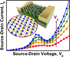
The damaging differential resistance (NDR) impact has been extensively investigated for the event of assorted digital gadgets. Aside from conventional semiconductor-based gadgets, two-dimensional (2D) transition steel dichalcogenide (TMD)-based field-effect transistors (FETs) have additionally lately exhibited NDR habits in a number of of their heterostructures. Nevertheless, to watch NDR within the type of monolayer MoS2, theoretical prediction has revealed that the fabric needs to be extra profoundly affected by sulfur (S) emptiness defects. On this work, monolayer MoS2 FETs with a certain amount of S-vacancy defects are fabricated utilizing three approaches, particularly chemical therapy (KOH resolution), bodily therapy (electron beam bombardment), and as-grown MoS2. Primarily based on systematic research on the correlation of the S-vacancies with each the system’s electron transport traits and spectroscopic evaluation, the NDR has been clearly noticed within the defect-engineered monolayer MoS2 FETs with an S-vacancy (VS) quantity of ∼5 ± 0.5%. Consequently, secure NDR habits will be noticed at room temperature, and its peak-to-valley ratio may also be successfully modulated through the gate electrical area and lightweight depth. By way of these outcomes, it’s envisioned that extra digital functions primarily based on defect-engineered layered TMDs will emerge within the close to future.