

Silicon carbide is turning into a significant participant on the quantum scene. Extensively utilized in specialised electronics items equivalent to LEDs and electrical automobiles, silicon carbide boasts versatility, vast industrial availability, and rising use in high-power electronics, making it a beautiful materials for quantum info science, whose impression is anticipated to be profound.
Drawing on physics on the atomic scale, applied sciences equivalent to quantum computer systems, networks, and sensors will possible revolutionize areas as various as communication, drug growth, and logistics within the coming a long time.
Now, scientists on the U.S. Division of Vitality’s (DOE) Argonne Nationwide Laboratory, DOE’s Sandia Nationwide Laboratories, and associate establishments have performed a complete examine on the creation of qubits—the basic models of quantum info processing—in silicon carbide.
In a first-of-its-kind examine, the Argonne and Sandia scientists harnessed cutting-edge nanoscale analysis instruments on the two labs and efficiently demonstrated a way for implanting qubits in silicon carbide with excessive precision. In addition they carried out state-of-the-art evaluation on how silicon carbide responds on the atomic scale to the qubits’ implantation.
Their high-precision investigations allow scientists to higher engineer quantum units for particular functions, whether or not to design ultraprecise sensors or construct an unhackable communication community.
The researchers’ work is printed within the journal Nanotechnology.
“We will higher perceive the molecular dynamics of the fabric past the standard hand-waving rationalization that we’re used to,” mentioned Argonne scientist Nazar Delegan, who’s the lead writer of the paper. “We additionally confirmed that we are able to create spatially localized qubits on this very related materials system, silicon carbide.”
Researchers are working to excellent the creation of qubits in silicon carbide. These qubits take the type of two side-by-side atom-sized holes, or vacancies, inside the silicon carbide crystal. Scientists name this pair of atomic holes a divacancy.
The group’s paper describes how they leverage a course of perfected at Sandia’s Middle for Built-in Nanotechnologies (CINT) to create the qubits. Utilizing one in all CINT’s nanoscale-materials instruments, scientists have been in a position to exactly implant silicon ions within the silicon carbide. The method knocks free atoms within the silicon carbide, creating divacancies within the materials.
The method allows scientists not solely to specify the precise variety of atoms to inject into the silicon carbide, but additionally to place the divacancies at a precision of roughly 25 nanometers. Such precision is essential for integrating quantum applied sciences into digital units.
“You do not have to go on a hunt to search out an atomic-scale emptiness in a bigger piece of fabric,” mentioned Michael Titze, Sandia scientist and the Sandia lead on the paper. “Through the use of the centered ion beam, you’ll be able to put the atom someplace, and another person can discover the emptiness inside a 100-nanometer scan. We’re making these things simpler to search out and, by extension, simpler to check and incorporate right into a sensible technological platform.”
Following the precision positioning of the qubits, scientists at Argonne annealed—or heated—the silicon carbide samples to boost the qubits’ properties and stabilize the silicon carbide crystal.
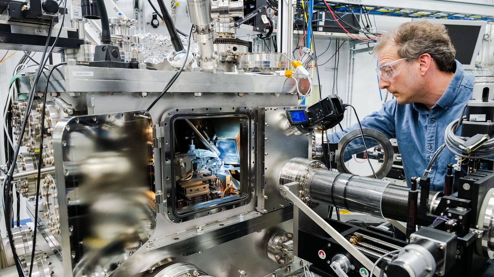
The staff then exactly mapped, for the primary time, the methods the divacancies fashioned inside the crystal and modifications in its nanoscale construction following the annealing course of. Their device for this characterization was Argonne’s highly effective Superior Photon Supply (APS), a DOE Workplace of Science person facility.
The APS is a huge, ring-shaped machine massive sufficient to encircle a sports activities stadium. It produces very vivid beams of X-rays to look deep inside supplies.
Researchers at Argonne’s Middle for Nanoscale Supplies (CNM), additionally a DOE Workplace of Science person facility, used CNM’s devoted X-ray beamline on the APS to check the mobilization and creation of divacancy qubits inside silicon carbide. What number of vacancies are fashioned once you alter the variety of implanted atoms? What occurs once you alter the atom’s vitality? How does the implantation have an effect on the construction of the silicon carbide?
“These impurities result in totally different crystal configurations, which result in pressure,” Titze mentioned. “How does the pressure get affected by these varied defects?”
To reply such questions, the staff centered a 25-nanometer-thin X-ray beam onto silicon carbide samples.
“You’ll be able to scan throughout your implanted materials, and at each single level, you are in a position to get the structural info of what is occurring,” Delegan mentioned. “So now you may have an X-ray approach of taking a look at these scales. You are in a position to say, “How was the crystal behaving earlier than, throughout, and after implantation?'”
Utilizing the CNM’s X-ray beamline on the APS, the group was in a position to picture modifications within the silicon carbide’s nanoscale construction with impressively excessive decision, detecting modifications at 1 half per million.
By combining the exact positioning of qubits utilizing Sandia’s CINT device and the exact imaging of their crystal atmosphere with Argonne’s APS and CNM, the staff takes a big step towards the creation of bespoke silicon carbide qubits, which is anticipated to result in higher customizability for quantum purposes.
Their work additionally provides to the ebook on silicon carbide qubits, empowering the scientific neighborhood to develop and tune their silicon-carbide-based quantum units in an intentional approach.
“This work allows all these quantum info science purposes the place you need to implant a really particular ion due to its helpful quantum properties,” Titze mentioned. “Now you can use this data of native pressure across the defects to engineer it in such a approach which you could make, say, a whole bunch of defects on a single chip speak to one another.”
The staff’s work is a testomony to inter-institutional collaboration.
“We at CINT present the potential for exact implantation of atoms,” Titze mentioned. “And our colleagues at CNM and Q-NEXT present a novel technique to make them really findable when they should search for them.”
The researchers will proceed to make use of the 2 labs’ nanoscale-materials instruments to characterize the dynamics of making qubits in silicon carbide.
“We have been in a position to exhibit the instruments’ sensitivities,” Delegan mentioned. “And the cool half is, with some additional experimental concerns, we should always be capable to begin to extract fascinating behaviors with these values.”
Extra info:
Nazar Delegan et al, Deterministic nanoscale quantum spin-defect implantation and diffraction pressure imaging, Nanotechnology (2023). DOI: 10.1088/1361-6528/acdd09
Offered by
Argonne Nationwide Laboratory
Quotation:
Scientists create qubits utilizing precision instruments of nanotechnology (2024, January 18)
retrieved 18 January 2024
from https://phys.org/information/2024-01-scientists-qubits-precision-tools-nanotechnology.html
This doc is topic to copyright. Aside from any truthful dealing for the aim of personal examine or analysis, no
half could also be reproduced with out the written permission. The content material is offered for info functions solely.
