
Semiconductor packaging applied sciences have developed from preliminary 1D PCB ranges to the cutting-edge 3D hybrid bonding packaging on the wafer degree. This development facilitates single-digit micronmeter interconnecting pitches, attaining over 1000 GB/s bandwidth with excessive vitality effectivity.
4 vital parameters form superior semiconductor packaging: energy, efficiency, space, and value:
- Energy: Enhancing energy effectivity by means of modern packaging applied sciences.
- Efficiency: Boosting bandwidth and lowering communication size by shortening interconnection pitch for extra enter/output (I/O) factors.
- Space: Bigger packaging space required for chips utilized in excessive efficiency computing areas, whereas smaller z-form issue are required for 3D integration.
- Price: Constantly lowering packaging prices by using various, extra reasonably priced supplies or enhancing manufacturing gear effectivity
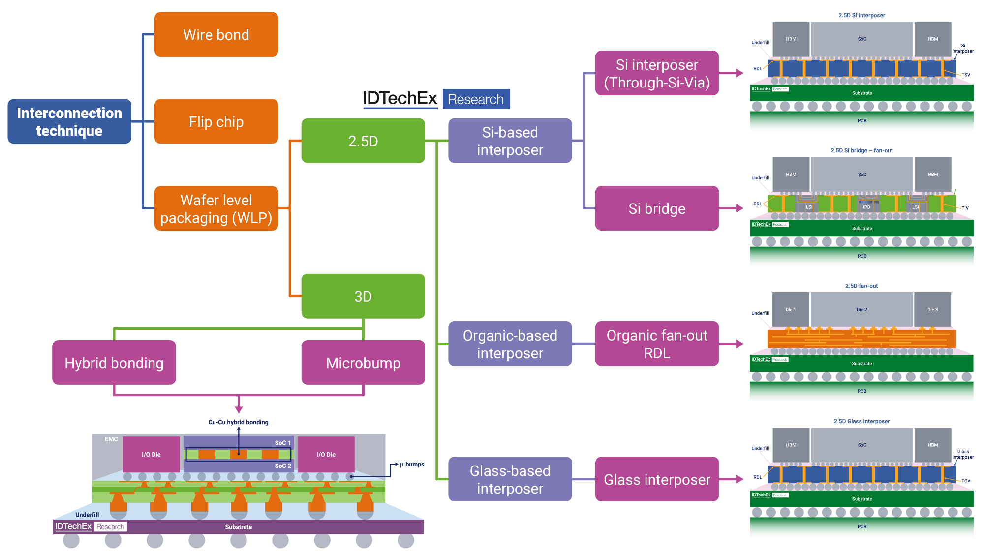
2.5D and 3D Packaging Know-how:
The two.5D and 3D packaging applied sciences embody numerous packaging strategies.
In 2.5D packaging, the selection of interposer materials categorizes it into Si-based, Natural-based, and glass-based interposers, as illustrated within the determine above. In the meantime, in 3D packaging, the evolution of microbump know-how goals for smaller pitch dimensions. Nonetheless, attaining single-digit pitch dimensions in the present day is made attainable by means of the adoption of hybrid bonding know-how, a technique that instantly connects Cu-Cu, signifying a major development within the subject.
Benefits and Drawbacks of Every Packaging Kind in Each 2.5D and 3D Configurations
2.5D
Si: There are two alternate options inside this class: Si interposer, using a full passive Si wafer, and Si bridge, which might take the type of a localized Si bridge in a fan-out based mostly molding compound or in a substrate with a cavity. The Si interposer, generally employed in 2.5D packaging for high-performance computing integration as a result of its means to facilitate the best routing options, faces challenges related to its value in each supplies and manufacturing in comparison with alternate options like natural supplies, and the packaging space limitation. To deal with this, the localized Si bridge kind is gaining prominence, strategically using Si the place positive options are important. Moreover, the Si bridge construction is predicted to see elevated use, notably in situations the place Si interposer faces limitations in space, pushing past the 4x or 5x reticle restrict.
Natural: Within the report, we particularly think about organic-based packaging that makes use of a fan-out molding compound reasonably than an natural substrate. Natural supplies, with the aptitude to regulate their dielectric fixed decrease than silicon, contribute to decrease RC delay within the package deal. Furthermore, these supplies current a more cost effective various to silicon. These benefits drive the emergence of organic-based 2.5D packaging. Nonetheless, a key downside lies within the challenges related to attaining the identical degree of interconnect characteristic discount as Si-based packages.
Glass: The glass-based method has gained vital curiosity following Intel’s unveiling of its glass-based take a look at automobile package deal earlier this yr. Glass possesses advantageous properties, together with tunable Coefficient of Thermal Enlargement (CTE), excessive dimensional stability, and a clean, flat floor. These traits place glass as a promising candidate for serving as an interposer, with routing options which have the potential to rival these provided by silicon. Nonetheless, the principle downside of glass lies in its immature ecosystem and a present lack of large-volume mass manufacturing functionality within the packaging trade. Nonetheless, because the ecosystem matures and manufacturing capabilities advance, the usage of glass-based applied sciences in semiconductor packaging might even see additional progress.
3D
Microbump: The well-established microbump know-how, based mostly on the Thermal Compression Bonding (TCB) course of, has a longstanding presence throughout numerous merchandise. Its roadmap entails ongoing scaling of bumping pitch. Nonetheless, a vital problem emerges as smaller solder ball sizes on this course of lead to heightened Intermetallic Compounds (IMCs) formation, diminishing conductivity and mechanical properties. Moreover, shut contact gaps could result in solder ball bridging, risking chip failure throughout reflow. With solder and IMCs exhibiting increased resistivity than copper, their use in high-performance part packaging faces limitations.
Hybrid bonding: Hybrid bonding entails creating everlasting interconnections by combining a dielectric materials (SiO2) with embedded metallic (Cu). With Cu-Cu hybrid bonding attaining pitches under 10 micrometers (usually round one-digit µm), benefits embody expanded I/O, elevated bandwidth, enhanced 3D vertical stacking, heightened energy effectivity, and decreased parasitics and thermal resistance because of the absence of underfill. Challenges embody manufacturing complexities and better prices related to this superior approach.
IDTechEx’s new report, “Superior Semiconductor Packaging 2024-2034: Forecasts, Applied sciences, Purposes“, completely explores the most recent improvements in semiconductor packaging know-how, protecting key technical developments, analyzing the worth chain, evaluating main gamers, and offering detailed market forecasts.
The report acknowledges the essential function of superior semiconductor packaging as the muse for next-generation ICs. It focuses on its purposes in key markets equivalent to AI and information facilities, 5G, autonomous autos, and shopper electronics. Leveraging IDTechEx’s experience in these sectors, the report delivers a complete understanding of the influence and future trajectory of superior semiconductor packaging in these vital fields.
Key Facets of This Report:
Exploring Know-how Developments and Producers in Superior Semiconductor Packaging:
- Discover superior semiconductor packaging evolution, addressing transistor IC challenges. Look at how chiplet ideas and heterogeneous integration propel superior packaging adoption.
- Analyze Packaging Applied sciences: Phase by interposer materials (Si, Glass, Natural), protecting roadmaps, benchmarks, purposes, gamers, and manufacturing obstacles.
- Firm Evaluation: In-depth examination of key firms, assessing options, clientele, purposes, and know-how roadmap.
- Key Markets: Present detailed overviews for vital markets – high-performance computing, autonomous autos, 5G, and shopper electronics.
- Case Research: Showcase numerous trade purposes of superior semiconductor packaging.
- Provide Chain & Fashions: Analyze provide chain dynamics and enterprise fashions on this evolving panorama.
10-year Granular Market Forecasts & Evaluation:
- Information Middle Server Unit Forecast 2023-2034 (Cargo)
- Information Middle CPU: Superior Semiconductor Packaging Forecast 2023-2034 (Cargo)
- Information Middle Accelerator: Semiconductor Packaging Forecast 2023-2034 (Cargo)
- 2.5D Semiconductor Packaging for L4+ Autonomous Autos 2023-2045
- 3D Semiconductor Packaging for L4+ Autonomous Autos 2023-2045
- Shopper Electronics Unit Gross sales Forecast 2023-2034 (Smartphones/Tablets/
Smartwatches/AR/VR/MR) - Superior Semiconductor Packaging Forecast for APE in Shopper Electronics 2023-2034
- International PC Cargo Forecast 2023-2034
- Superior Semiconductor Packaging in PC Forecast 2023-2034
- 5G Radios by MIMO Measurement Unit Forecast 2023-2034
- Superior Semiconductor Packaging for 5G RAN Networks 2023-2034
Supply: https://www.idtechex.com/
