
(Nanowerk Information) Substitutional doping from international parts stands out as a most popular methodology for exactly tailoring the digital band construction, conduction sort, and service focus of pristine supplies. Within the realm of three-dimensional (3D) monocrystalline silicon, as an example, the introduction of boron (B) and nitrogen (N) atoms as acceptor and donor dopants, respectively, has confirmed extremely efficient in enhancing service mobility. This enchancment positions silicon for superior purposes in built-in circuits.
Increasing into the realm of two-dimensional (2D) semiconductors, molybdenum disulfide (MoS2) holds immense potential for future optoelectronic units. Nonetheless, the controllable doping methods for 2D supplies and their potential software instructions necessitate additional exploration. As a brand new frontier in supplies science, the search for optimum doping methodologies in 2D supplies continues to unfold, paving the best way for unprecedented developments within the area of optoelectronics.
Researchers led by Anlian Pan, Dong Li and Shengman Li from Hunan College, China, are devoted to pioneering the synthesis of large-area, high-quality, and low-defect-density two-dimensional semiconductors. Their analysis focuses on unraveling the photoelectric properties of those supplies and exploring their potential in future gadget purposes.
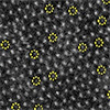
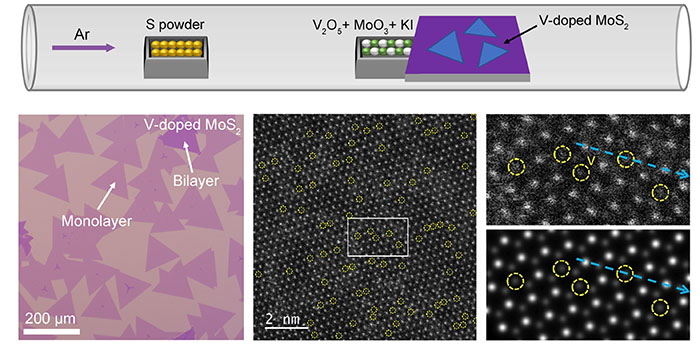 V-doped MoS2 monolayer is achieved by way of chemical vapor deposition methodology. (©Frontiers of Optoelectronics)
Constructing on the muse of getting ready high-mobility pure MoS2, the researchers delved into the realm of international substitutional doping, introducing vanadium (V) atoms. Their strategy aimed to fine-tune the switch traits of MoS2 by various the V doping focus. Notably, their investigations revealed that V-doped MoS2 monolayers with low doping concentrations exhibited enhanced B-exciton emission, showcasing promise for purposes in broadband photodetectors.
This work was printed in Frontiers of Optoelectronics (“Vapor development of V-doped MoS2 monolayers with enhanced B-exciton emission and broad spectral response”). This analysis contributes invaluable insights to the evolving panorama of two-dimensional semiconductors and their potential affect on optoelectronic applied sciences.
V-doped MoS2 monolayer is achieved by way of chemical vapor deposition methodology. (©Frontiers of Optoelectronics)
Constructing on the muse of getting ready high-mobility pure MoS2, the researchers delved into the realm of international substitutional doping, introducing vanadium (V) atoms. Their strategy aimed to fine-tune the switch traits of MoS2 by various the V doping focus. Notably, their investigations revealed that V-doped MoS2 monolayers with low doping concentrations exhibited enhanced B-exciton emission, showcasing promise for purposes in broadband photodetectors.
This work was printed in Frontiers of Optoelectronics (“Vapor development of V-doped MoS2 monolayers with enhanced B-exciton emission and broad spectral response”). This analysis contributes invaluable insights to the evolving panorama of two-dimensional semiconductors and their potential affect on optoelectronic applied sciences.
