| Jan 03, 2024 |
|
(Nanowerk Information) Coal is an ample useful resource in the US that has, sadly, contributed to local weather change by its use as a fossil gas. Because the nation transitions to different technique of power manufacturing, it is going to be essential to contemplate and reevaluate coal’s financial position. A joint analysis effort from the College of Illinois Urbana-Champaign, the Nationwide Vitality Expertise Laboratory, Oak Ridge Nationwide Laboratory and the Taiwan Semiconductor Manufacturing Firm has proven how coal can play a significant position in next-generation digital gadgets.
|
Key Takeaways
|
|
Coal’s potential in superior electronics is highlighted by its transformation into high-purity, atomically skinny supplies.
Progressive processing strategies can convert coal into carbon dots, forming the premise for ultra-thin, energy-efficient electronics.
These coal-derived supplies are perfect for establishing next-gen electronics like two-dimensional transistors and memristors, providing enhanced efficiency.
The analysis demonstrates coal’s functionality to behave as an environment friendly insulator in digital gadgets, lowering power consumption and enhancing pace.
Collaboration continues to scale up these applied sciences for industrial implementation, with vital curiosity from the semiconductor business.
|
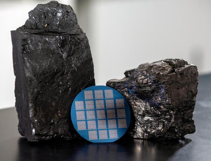 |
| A wafer containing memristors fabricated with high-quality two-dimensional carbon processed from bituminous Blue Gem coal mined in southeastern Kentucky, two samples of that are proven right here. (Picture: College of Illinois Urbana-Champaign)
|
The Analysis
|
|
“Coal is normally regarded as one thing cumbersome and soiled, however the processing strategies we’ve developed can remodel it into high-purity supplies simply a few atoms thick,” stated Qing Cao, a U. of I. supplies science & engineering professor and a co-lead of the collaboration. “Their distinctive atomic constructions and properties are perfect for making a number of the smallest attainable electronics with efficiency superior to state-of-the artwork.”
|
|
A course of developed by the NETL first converts coal char into nanoscale carbon disks referred to as “carbon dots” that the U. of I. analysis group demonstrated might be related to kind atomically skinny membranes for functions in each two-dimensional transistors and memristors, applied sciences that might be important to establishing extra superior electronics.
|
|
These outcomes are reported within the journal Communications Engineering (“Ultrathin Quasi-2D Amorphous Carbon Dielectric Ready from Answer Precursor for Nanoelectronics”).
|
Excellent for 2D electronics
|
|
Within the ongoing seek for smaller, quicker and extra environment friendly electronics, the ultimate step might be gadgets made with supplies only one or two atoms thick. It’s unimaginable for gadgets to be smaller than this restrict, and their small scale usually makes them function a lot faster and eat far much less power. Whereas ultrathin semiconductors have been extensively studied, it’s also essential to have atomically skinny insulators – supplies that block electrical currents – to assemble working digital gadgets like transistors and memristors.
|
|
Atomically skinny layers of carbon with disordered atomic constructions can perform as a wonderful insulator for establishing two-dimensional gadgets. The researchers within the collaboration have proven that such carbon layers might be fashioned from carbon dots derived from coal char. To show their capabilities, the U. of I. group led by Cao developed two examples of two-dimensional gadgets.
|
|
“It’s actually fairly thrilling, as a result of that is the primary time that coal, one thing we usually see as low-tech, has been immediately linked to the slicing fringe of microelectronics,” Cao stated.
|
Transistor dielectric
|
|
Cao’s group used coal-derived carbon layers because the gate dielectric in two-dimensional transistors constructed on the semimetal graphene or semiconductor molybdenum disulfide to allow greater than two occasions quicker gadget working pace with decrease power consumption. Like different atomically skinny supplies, the coal-derived carbon layers don’t possess “dangling bonds,” or electrons that aren’t related to a chemical bond. These websites, that are ample on the floor of typical three-dimensional insulators, alter their electrical properties by successfully functioning as “traps,” slowing down the transport of cellular prices and thus the transistor switching pace.
|
|
Nonetheless, not like different atomically skinny supplies, the brand new coal-derived carbon layers are amorphous, that means that they don’t possess a daily, crystalline construction. They subsequently don’t have boundaries between totally different crystalline areas that function conduction pathways resulting in “leakage,” the place undesired electrical currents stream by the insulator and trigger substantial extra energy consumption throughout gadget operations.
|
Memristor filament
|
|
One other utility Cao’s group thought of is memristors – digital parts able to each storing and working on knowledge to tremendously improve the implementation of AI know-how. These gadgets retailer and symbolize knowledge by modulating a conductive filament fashioned by electrochemical reactions between a pair of electrodes with the insulator sandwiched in between.
|
|
The researchers discovered that the adoption of ultrathin coal-derived carbon layers because the insulator permits the quick formation of such filament with low power consumption to allow excessive gadget working pace with low energy. Furthermore, atomic measurement rings in these coal-derived carbon layers confine the filament to reinforce the reproducible gadget operations for enhanced knowledge storage constancy and reliability.
|
From analysis to manufacturing
|
|
The brand new gadgets developed by the Cao group present proof-of-principle for the usage of coal-derived carbon layers in two-dimensional gadgets. What stays is to indicate that such gadgets might be manufactured on massive scales.
|
|
“The semiconductor business, together with our collaborators at Taiwan Semiconductor, may be very within the capabilities of two-dimensional gadgets, and we’re attempting to meet that promise,” Cao stated. “Over the following few years, the U. of I. will proceed to collaborate with NETL to develop a fabrication course of for coal-based carbon insulators that may be applied in industrial settings.”
|

