
For those who had been a reader of IEEE Spectrum in 2023 with an curiosity in semiconductors, this checklist of the highest tales says some attention-grabbing issues about you. As an example, you appreciated scandal and pace. However you’re additionally a discerning and forward-looking particular person. You needed to know what the way forward for Moore’s Regulation is and who can be making it occur. You additionally needed to understand how semiconductors will play a component in combating local weather change.
We’re already supplying you with a style of the subsequent yr in semiconductors, and we are able to’t wait to see what you learn most in 2024.
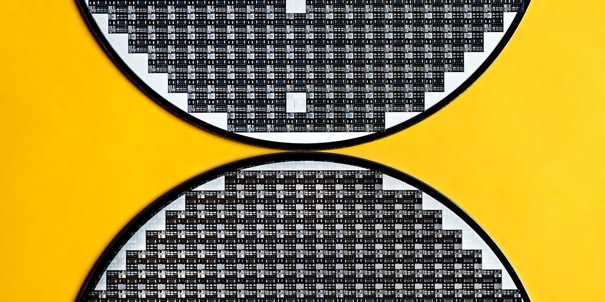
1. Ending an Ugly Chapter in Chip Design

Chung-Kuan Cheng et al.
In 2022, a schism within the chip design world and at Google erupted into the open. At difficulty was a reinforcement-learning AI system that Google makes use of to do a key step in laying out chunks of logic and reminiscence for its AI accelerator chips, or TPUs. In analysis revealed in Nature in 2021, Google claimed it beat high tutorial algorithms and human chip designers at discovering the optimum layouts. A rival group at Google responded that it didn’t, however the firm wouldn’t publish the rival’s outcomes. When a model was leaked forward of a serious convention, issues obtained ugly.
A yr later, a bunch led by IEEE Fellow Andrew Kahng reported analysis he stated was meant to get the neighborhood previous the disagreeable episode. Kahng’s analysis largely backed the rival group’s tackle issues. It has since led to an editorial expression of concern from Nature, and Kahng has retracted the editorial that initially accompanied Google’s paper. However the search big nonetheless backs its AI. As just lately as August 2023, Jeff Dean, chief scientist at Google DeepMind, stated that in comparison with different strategies the TPU group had accessible, 26 of the TPU’s 37 blocks had higher performing layouts due to the AI, and seven of 37 carried out equally properly.
2. U.S. Universities Are Constructing a Semiconductor Workforce
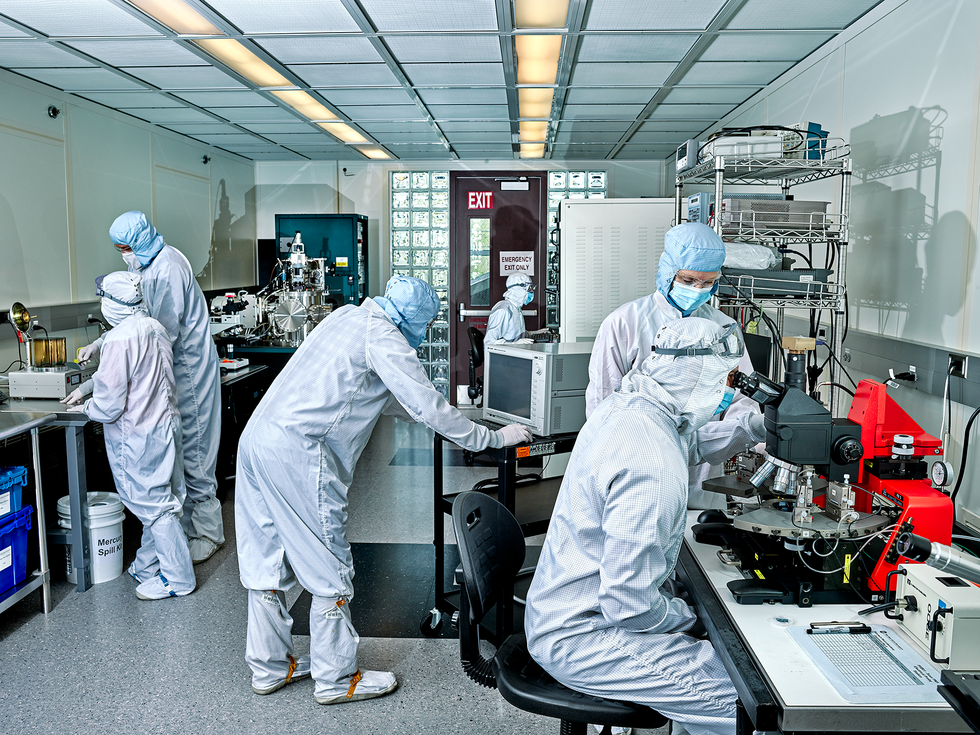
Peter Adams
With the U.S. CHIPS and Science Act set to pump tens of billions of {dollars} into chip manufacturing in the USA, the query has come up: “Who’s gonna work in these new fabs?” As long-time contributor Prachi Patel studies, universities throughout the USA, particularly these close to fab development tasks, are revamping their semiconductor schooling choices in response. The hope is to steer proficient college students away from the attract of AI and different scorching fields and steer them towards making the chips that make AI occur.
3. Thermal Transistors Can Deal with Warmth With No Transferring Components
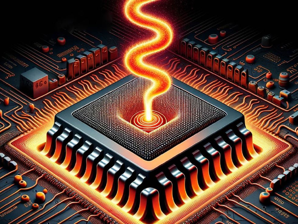
H-Lab/UCLA
In November, researchers from College of California, Los Angeles reported the invention of a thermal transistor, the primary solid-state gadget that makes use of an digital sign to regulate the circulation of warmth. Warmth removing has been a long-standing restrict on processor efficiency, and it’s solely going to get harder as processors turn into collections of 3D-stacked chiplets. Even right this moment’s superior strategies are sluggish to react to adjustments in chip temperature when in comparison with a thermal transistor, which may change warmth conductance on and off as shortly as 1 megahertz.
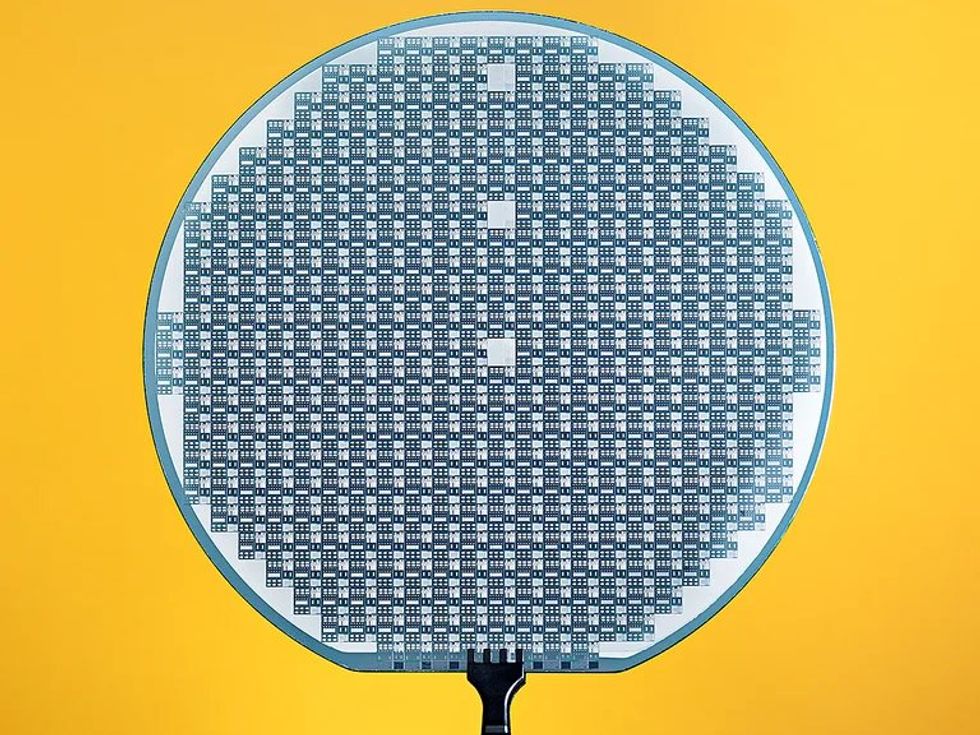
4. Contained in the Moore’s Regulation Machine

ASML
Excessive ultraviolet lithography was many years within the making, solely coming into common service a number of years in the past to print nanometer-scale patterns on essentially the most superior chips. It’s already time for an improve. As engineers at ASML defined in Spectrum‘s August difficulty, the model of the expertise in use now’s restricted to creating patterns with a decision of concerning the wavelength of its gentle, 13.5 nanometers. To get under that restrict, engineers needed to make some main adjustments to the system’s optics and repair all of the knock-on issues that adopted. By the way, this isn’t the one enchancment to EUV coming. New expertise, resembling a gasoline cell working in reverse, will make the expertise greener. You possibly can hear about each in this episode of IEEE Spectrum’s Fixing the Future podcast.
5. Gallium Nitride and Silicon Carbide Combat for Inexperienced Tech Domination
 Peter Adams
We fear increasingly more concerning the carbon footprint of semiconductor manufacturing, however this story was truly a win for the local weather. Silicon carbide and gallium nitride energy semiconductors are each extra environment friendly than their silicon counterparts. The query IEEE Spectrum sought to reply was: Which of those vast bandgap semiconductors works finest when? The reply is difficult however fascinating. One factor is obvious, each these semiconductors will maintain a number of carbon from coming into the ambiance.
6. Intel Is All-In on Again-Aspect Energy Supply
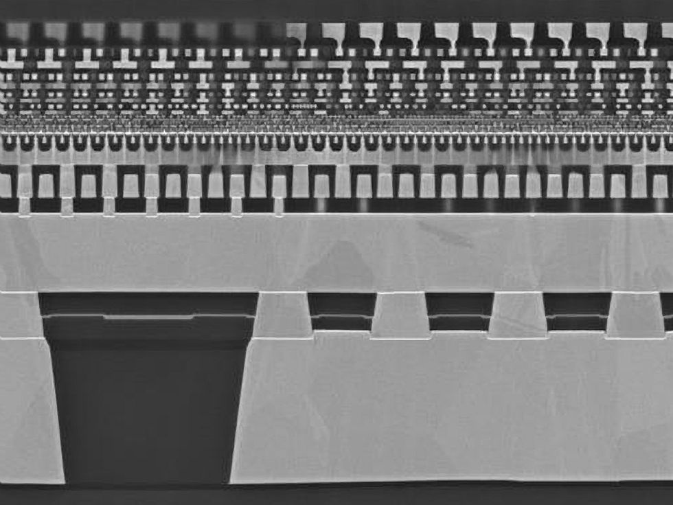
Chipmakers plan a giant change within the structure of interconnects in high-end processors. Because the IC was invented, the entire steel that connects transistors was shaped above the silicon floor. That’s labored properly for many years, however it’s going to have to return to an finish. There’s a elementary stress between what data-carrying interconnects want and what power-carrying interconnects need. Mainly, much less energy is misplaced if the interconnects carrying it are quick and vast. So researchers hatched a scheme to maneuver the ability supply community to the underside of the silicon, the place steel strains may very well be saved broad and conductive. That leaves extra room to higher pack within the data-carrying strains above. Intel was the primary chipmaker to announce that it could manufacture chips utilizing back-side energy supply, a tech it calls PowerVia. In June, the corporate shared outcomes exhibiting that, by itself, PowerVia results in a few 6 % efficiency enhance, which is about half what you sometimes get from a serious scale down of transistors. Intel will probably be making a CPU utilizing the mix of PowerVia and new transistors it calls RibbonFETs in 2024.
7. 4 Methods to Put Lasers on Silicon
 Emily Cooper
Silicon is nice for many issues. Making lasers will not be one in all them. However having a laser on a silicon chip solves a number of awkward integration issues that might assist pace knowledge between processors and different chips. So engineers have been developing with sensible methods to combine lasers fabricated from compound semiconductors onto silicon wafers, and do it in a means that’s manufacturable and comparatively low cost. We confirmed you 4 of them, ranked from essentially the most mature to the farthest out.
8. Particle Accelerator on a Chip Hits Penny-Dimension
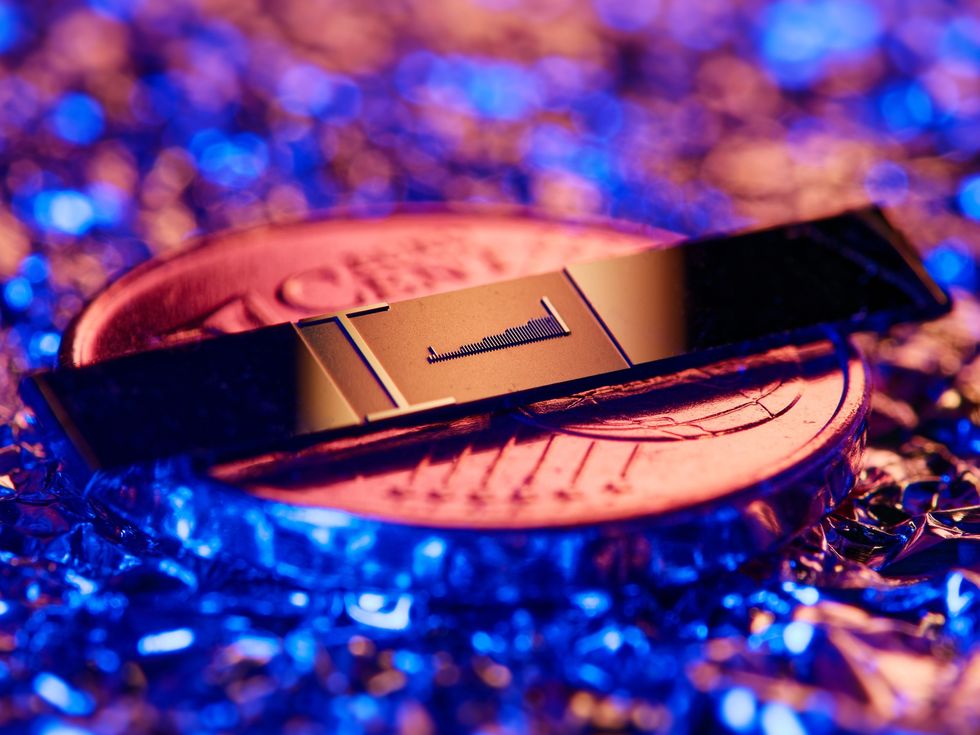
FAU/Laserphysics/Litzel/Kraus
Few applied sciences have variations which might be each the scale of a metropolis and the scale of small coin. However now particle accelerators could make that declare. As a substitute of utilizing electrical fields to spice up the pace of electrons alongside a protracted monitor, scientists in Germany used gentle to zip them by way of a groove simply nanometers vast and 0.5 millimeters lengthy. At that scale the electrical area that speeds the electrons alongside comes from the sunshine’s oscillating electrical area. Electrons went 40 % quicker beneath the accelerator’s affect. The scientists hope they’ll sometime zap them to speeds helpful for medical analysis and different functions.
9. Researchers Uncover the Quickest Semiconductor But
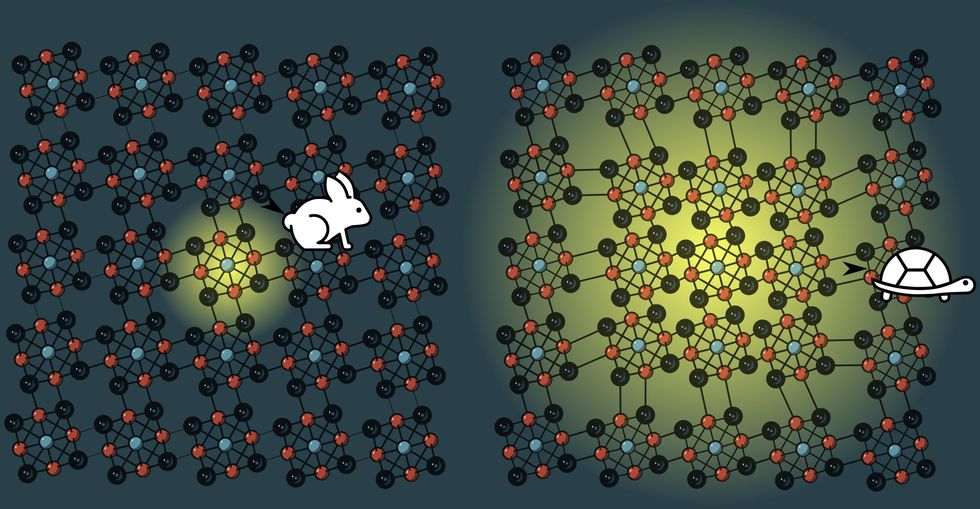
Jack Tulyag/Columbia College
What has 6 rhenium atoms, 8 seleniums, and 12 chlorines? The quickest semiconductor but found, that’s what. This molecule kinds superclusters that act like one massive atom however with properties no single a type of parts has. The key to its pace lies the conduct of phonons, quasiparticles shaped from vibrations in a strong. Often phonons sluggish issues down, partly by interfering with excitons, sure pairs of electrons and positively charged holes. As a substitute of knocking excitons round, phonons on this molecule bind to them to create a brand new quasiparticle that circulation freely by way of the semiconductor at twice the pace of electrons. Too unhealthy rhenium is likely one of the rarest parts on Earth.
10. The Sensible Energy of Fusing Photons
 Chad Hagen
Silicon photo voltaic cells are comparatively low cost and plentiful, however they miss out on a number of vitality in daylight. Mainly, no colour of sunshine with an vitality lower than silicon’s bandgap will get used. However what if we may flip these colours into silicon’s most popular hues? Researchers at Stanford defined simply how that’s executed. Via an advanced means of exchanging electrons between a number of molecules and vitality states, they’ve discovered a method to flip two ineffective photons into one helpful one. The implications for photovoltaics may very well be monumental.
From Your Website Articles
Associated Articles Across the Internet
