
Quantum computing is a devilishly complicated expertise, with many technical hurdles impacting its growth. Of those challenges two important points stand out: miniaturization and qubit high quality.
IBM has adopted the superconducting qubit street map of reaching a 1,121-qubit processor by 2023, resulting in the expectation that 1,000 qubits with right now’s qubit type issue is possible. Nonetheless, present approaches would require very giant chips (50 millimeters on a aspect, or bigger) on the scale of small wafers, or using chiplets on multichip modules. Whereas this strategy will work, the intention is to realize a greater path towards scalability.
Now researchers at MIT have been in a position to each cut back the dimensions of the qubits and accomplished so in a approach that reduces the interference that happens between neighboring qubits. The MIT researchers have elevated the variety of superconducting qubits that may be added onto a tool by an element of 100.
“We’re addressing each qubit miniaturization and high quality,” stated William Oliver, the director for the Middle for Quantum Engineering at MIT. “Not like typical transistor scaling, the place solely the quantity actually issues, for qubits, giant numbers are usually not ample, they need to even be high-performance. Sacrificing efficiency for qubit quantity just isn’t a helpful commerce in quantum computing. They have to go hand in hand.”
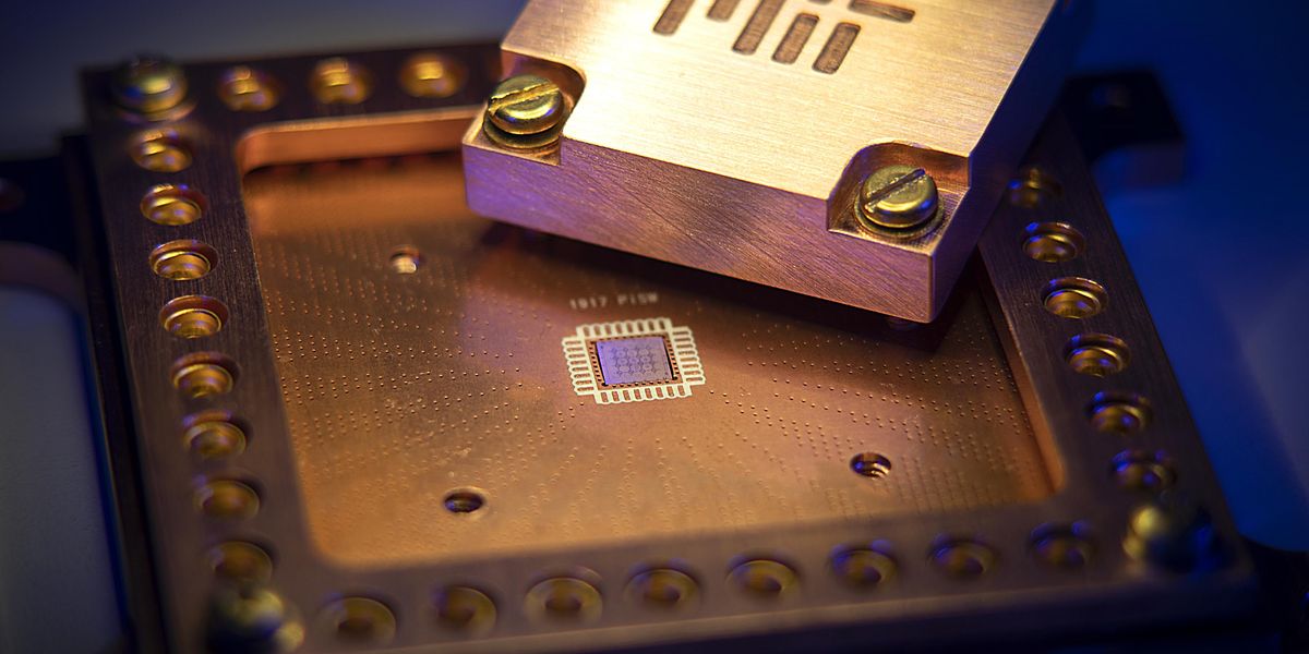
The important thing to this massive enhance in qubit density and discount of interference comes right down to using two-dimensional supplies, particularly the 2D insulator hexagonal boron nitride (hBN). The MIT researchers demonstrated that a couple of atomic monolayers of hBN might be stacked to type the insulator within the capacitors of a superconducting qubit.
Identical to different capacitors, the capacitors in these superconducting circuits take the type of a sandwich during which an insulator materials is sandwiched between two metallic plates. The massive distinction for these capacitors is that the superconducting circuits can function solely at extraordinarily low temperatures—lower than 0.02 levels above absolute zero (-273.15 °C).
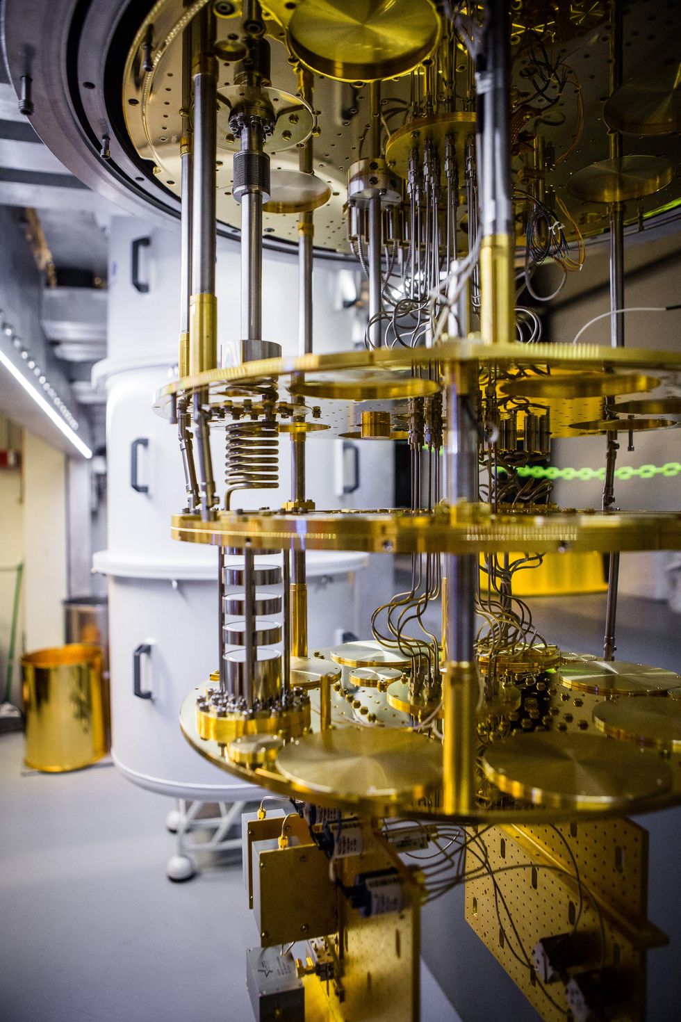 Superconducting qubits are measured at temperatures as little as 20 millikelvin in a dilution fridge.Nathan Fiske/MIT
In that surroundings, insulating supplies which can be accessible for the job, resembling PE-CVD silicon oxide or silicon nitride, have fairly a couple of defects which can be too lossy for quantum computing purposes. To get round these materials shortcomings, most superconducting circuits use what are known as coplanar capacitors. In these capacitors, the plates are positioned laterally to 1 one other, relatively than on prime of each other.
Consequently, the intrinsic silicon substrate under the plates and to a smaller diploma the vacuum above the plates function the capacitor dielectric. Intrinsic silicon is chemically pure and due to this fact has few defects, and the big measurement dilutes the electrical discipline on the plate interfaces, all of which results in a low-loss capacitor. The lateral measurement of every plate on this open-face design finally ends up being fairly giant (usually 100 by 100 micrometers) in an effort to obtain the required capacitance.
In an effort to maneuver away from the big lateral configuration, the MIT researchers launched into a seek for an insulator that has only a few defects and is suitable with superconducting capacitor plates.
“We selected to check hBN as a result of it’s the most generally used insulator in 2D materials analysis as a consequence of its cleanliness and chemical inertness,” stated colead creator Joel Wang, a analysis scientist within the Engineering Quantum Techniques group of the MIT Analysis Laboratory for Electronics.
On both aspect of the hBN, the MIT researchers used the 2D superconducting materials, niobium diselenide. One of many trickiest features of fabricating the capacitors was working with the niobium diselenide, which oxidizes in seconds when uncovered to air, in response to Wang. This necessitates that the meeting of the capacitor happen in a glove field stuffed with argon gasoline.
Whereas this might seemingly complicate the scaling up of the manufacturing of those capacitors, Wang doesn’t regard this as a limiting issue.
“What determines the standard issue of the capacitor are the 2 interfaces between the 2 supplies,” stated Wang. “As soon as the sandwich is made, the 2 interfaces are “sealed” and we don’t see any noticeable degradation over time when uncovered to the ambiance.”
This lack of degradation is as a result of round 90 % of the electrical discipline is contained inside the sandwich construction, so the oxidation of the outer floor of the niobium diselenide doesn’t play a major function anymore. This in the end makes the capacitor footprint a lot smaller, and it accounts for the discount in cross speak between the neighboring qubits.
“The primary problem for scaling up the fabrication would be the wafer-scale development of hBN and 2D superconductors like [niobium diselenide], and the way one can do wafer-scale stacking of those movies,” added Wang.
Wang believes that this analysis has proven 2D hBN to be a very good insulator candidate for superconducting qubits. He says that the groundwork the MIT workforce has accomplished will function a street map for utilizing different hybrid 2D supplies to construct superconducting circuits.
