| Dec 22, 2023 |
|
(Nanowerk Information) Researchers at Nagoya College in Japan have used synthetic intelligence to find a brand new methodology for understanding small defects known as dislocations in polycrystalline supplies, supplies broadly utilized in info gear, photo voltaic cells, and digital gadgets, that may cut back the effectivity of such gadgets.
|
|
The findings had been revealed within the journal Superior Supplies (“Multicrystalline Informatics Utilized to Multicrystalline Silicon for Unraveling the Microscopic Root Explanation for Dislocation Era”).
|
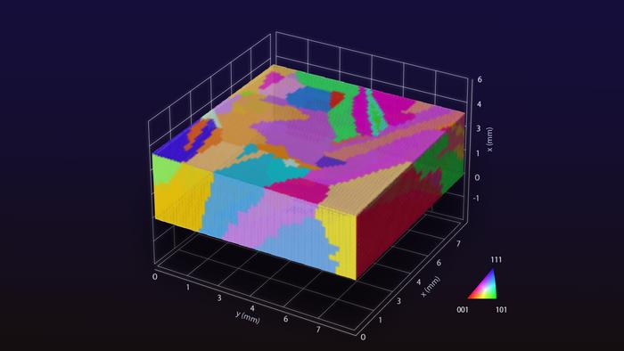 |
| Researchers used 3D mannequin created by AI to grasp complicated polycrystalline supplies which might be utilized in our on a regular basis digital gadgets.(Picture: Kenta Yamakoshi)
|
|
Virtually each machine that we use in our fashionable lives has a polycrystal part. Out of your smartphone to your laptop to the metals and ceramics in your automotive. Regardless of this, polycrystalline supplies are powerful to make the most of due to their complicated constructions. Together with their composition, the efficiency of a polycrystalline materials is affected by its complicated microstructure, dislocations, and impurities.
|
|
A serious drawback for utilizing polycrystals in trade is the formation of tiny crystal defects brought on by stress and temperature adjustments. These are often called dislocations and might disrupt the common association of atoms within the lattice, affecting electrical conduction and general efficiency. To scale back the probabilities of failure in gadgets that use polycrystalline supplies, you will need to perceive the formation of those dislocations.
|
|
A group of researchers at Nagoya College, led by Professor Noritaka Usami and together with Lecturer Tatsuya Yokoi and Affiliate Professor Hiroaki Kudo and collaborators, used a brand new AI to analyse picture knowledge of a cloth broadly utilized in photo voltaic panels, known as polycrystalline silicon. The AI created a 3D mannequin in digital area, serving to the group to determine the areas the place dislocation clusters had been affecting the fabric’s efficiency.
|
|
After figuring out the areas of the dislocation clusters, the researchers used electron microscopy and theoretical calculations to grasp how these areas shaped. They revealed stress distribution within the crystal lattice and located staircase-like constructions on the boundaries between the crystal grains. These constructions seem to trigger dislocations throughout crystal development. “We discovered a particular nanostructure within the crystals related to dislocations in polycrystalline constructions,” Usami mentioned.
|
|
Together with its sensible implications, this research might have vital implications for the science of crystal development and deformation as effectively. The Haasen-Alexander-Sumino (HAS) mannequin is an influential theoretical framework used to grasp the conduct of dislocations in supplies. However Usami believes that they’ve found dislocations that the Haasen-Alexander-Sumino mannequin missed.
|
|
One other shock was to comply with quickly after, as when the group calculated the association of the atoms in these constructions, they discovered unexpectedly giant tensile bond strains alongside the sting of the staircase-like constructions that triggered dislocation technology.
|
|
As defined by Usami, “As specialists who’ve been learning this for years, we had been amazed and excited to lastly see proof of the presence of dislocations in these constructions. It means that we will management the formation of dislocation clusters by controlling the route through which the boundary spreads.”
|
|
“By extracting and analyzing the nanoscale areas via polycrystalline supplies informatics, which mixes experiment, concept, and AI, we made this clarification of phenomena in complicated polycrystalline supplies potential for the primary time,” Usami continued. “This analysis illuminates the trail in the direction of establishing common pointers for high-performance supplies and is anticipated to contribute to the creation of revolutionary polycrystalline supplies. The potential affect of this analysis extends past photo voltaic cells to every thing from ceramics to semiconductors. Polycrystalline supplies are broadly utilized in society, and the improved efficiency of those supplies has the potential to revolutionize society.”
|

