

Researchers from Penn State have demonstrated a novel technique of 3D integration utilizing 2D supplies. This development, detailed of their latest examine, addresses the rising problem of becoming extra transistors into more and more smaller areas, a key concern within the semiconductor trade as gadgets proceed to shrink in measurement whereas requiring enhanced performance
The variety of transistors on a chip will double each two years, in keeping with Moore’s Regulation, a key scaling idea for digital gadgets, guaranteeing rising processing energy—however there’s a restrict.
As we speak’s strongest processors have roughly 50 billion transistors in an space the scale of a single thumbnail. In keeping with Penn State consultants, the job of becoming much more transistors into that tight area has grown more and more robust.
Saptarshi Das, an Affiliate Professor of Engineering Science and Mechanics and co-corresponding creator of the examine, and his colleagues suggest an answer in a examine revealed on January 10th, 2023 within the scientific journal Nature: easily integrating 3D integration with 2D supplies.
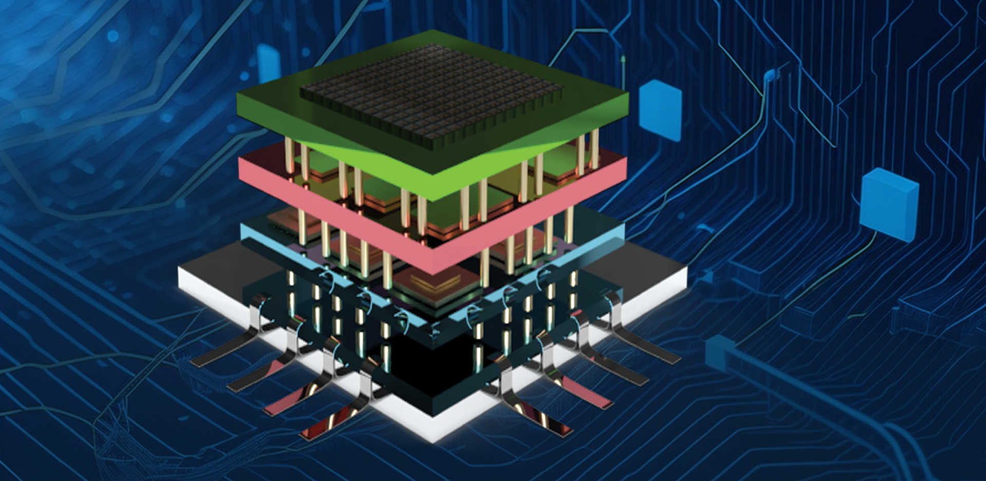
Inside the semiconductor trade, 3D integration refers back to the vertical stacking of a number of layers of semiconductor elements. This technique not solely makes it simpler to suit extra silicon-based transistors onto a pc chip—a course of referred to as “Extra Moore”—nevertheless it additionally makes it doable to make use of transistors product of two-dimensional supplies to include completely different functionalities inside completely different layers of the stack—an idea referred to as “Greater than Moore.”
By way of the work described within the examine, Saptarshi and the workforce present that there are sensible methods to perform Extra Moore and Greater than Moore by monolithic 3D integration, along with scaling present know-how. As an alternative of stacking individually manufactured layers as previously, researchers that use monolithic 3D integration assemble the gadgets straight on high of one another.
Monolithic 3D integration presents the very best density of vertical connections because it doesn’t depend on bonding of two pre-patterned chips — which might require microbumps the place two chips are bonded collectively — so you’ve extra space to make connections.
Najam Sakib, Examine Co-Creator and Graduate Analysis Assistant, Pennsylvania State College
Nevertheless, Darsith Jayachandran, a graduate analysis assistant in engineering science and mechanics and co-corresponding creator of the examine, factors out that monolithic 3D integration presents substantial issues as a result of conventional silicon elements would soften at processing temperatures.
One problem is the method temperature ceiling of 450 levels Celsius (C) for back-end integration for silicon-based chips — our monolithic 3D integration strategy drops that temperate considerably to lower than 200 C. Incompatible course of temperature budgets make monolithic 3D integration difficult with silicon chips, however 2D supplies can stand up to temperatures wanted for the method.
Darsith Jayachandran, Examine Co-Corresponding Creator and Graduate Analysis Assistant, Pennsylvania State College
Though the researchers employed pre-existing methodologies, they’re the primary to perform monolithic 3D integration at this scale by using transition steel dichalcogenides, a sort of 2D semiconductor, to create 2D transistors.
It’s about including new and helpful options to our digital gadgets, like higher sensors, improved battery administration or different particular capabilities, to make our devices smarter and extra versatile.
Muhtasim Ul Karim Sadaf, Graduate Analysis Assistant, Pennsylvania State College
Extra energy-efficient computing was additionally made doable by the 3D integration’s skill to vertically stack the gadgets, which resolved an surprising challenge for such tiny elements as transistors on a pc chip: distance.
By stacking gadgets vertically on high of one another, you are lowering the gap between gadgets, and due to this fact, you are lowering the lag and in addition the ability consumption.
Rahul Pendurthi, Examine Co-Corresponding Creator and Graduate Analysis Assistant, Pennsylvania State College
The researchers have been capable of get hold of “Extra Moore” by decreasing the gap between gadgets. Moreover, the researchers happy the “Greater than Moore” requirement by using transistors constructed of two-dimensional supplies.
The particular optical and electrical traits of 2D supplies, reminiscent of their mild sensitivity, make them good to be used as sensors. The researchers claimed that that is useful given the rising variety of edge gadgets and linked devices, reminiscent of wi-fi residence climate sensors and cell telephones that acquire information on the “edge” of a community.
Muhtasim Ul Karim Sadaf, graduate analysis assistant in engineering science and mechanics and co-author of the examine, acknowledged, “Extra Than Moore’ refers to an idea within the tech world the place we aren’t simply making laptop chips smaller and quicker, but additionally with extra functionalities. It’s about including new and helpful options to our digital gadgets, like higher sensors, improved battery administration or different particular capabilities, to make our devices smarter and extra versatile.”
The researchers famous that there are a number of extra advantages to utilizing 2D gadgets for 3D integration. Superior service mobility is likely one of the traits of semiconductor supplies that describes the best way {an electrical} cost is conveyed. One other is being extraordinarily skinny, which permits the researchers so as to add extra computational energy and extra transistors to every layer of the 3D integration.
The examine demonstrated 3D integration at a big scale, characterizing tens of 1000’s of gadgets, in distinction to typical educational analysis that makes use of small-scale prototypes. Das claims that this accomplishment closes the information hole between teachers and enterprise and will open the best way for extra collaborations wherein companies use Penn State’s assets and expertise in 2D supplies.
The provision of high-quality, wafer-scale transition steel dichalcogenides produced by scientists at Penn State’s Two-Dimensional Crystal Consortium (2DCC-MIP), a nationwide consumer facility, and US Nationwide Science Basis (NSF) Supplies Innovation Platform, made the scaling development doable.
Charles Ying, Program Director for NSF’s Supplies Innovation Platforms, added, “This breakthrough demonstrates but once more the important position of supplies analysis as the inspiration of the semiconductor trade and US competitiveness. Years of effort by Penn State’s Two-Dimensional Crystal Consortium to enhance the standard and measurement of 2D supplies have made it doable to realize 3D integration of semiconductors at a measurement that may be transformative for electronics.”
Das contends that that is just the start of technological progress.
He famous, “Our skill to display, at wafer scale, an enormous variety of gadgets reveals that we now have been capable of translate this analysis to a scale which will be appreciated by the semiconductor trade. We’ve put 30,000 transistors in every tier, which can be a report quantity. This places Penn State in a really distinctive place to guide among the work and associate with the U.S. semiconductor trade in advancing this analysis.”
Together with Das, Jayachandran, Pendurthi, Sadaf and Sakib, different authors embrace Andrew Pannone, Doctoral Pupil in Engineering Science and Mechanics; Chen Chen, Assistant Analysis Professor in 2DCC-MIP; Ying Han, Postdoctoral Researcher in Mechanical Engineering; Nicholas Trainor, doctoral scholar in supplies science and engineering; Shalini Kumari, Postdoctoral Scholar; Thomas McKnight, doctoral scholar in supplies science and engineering; Joan Redwing, Director of the 2DCC-MIP and Distinguished Professor of Supplies Science and Engineering and of Electrical Engineering; and Yang Yang, Assistant Professor of Engineering Science and Mechanics.
The examine was supported by the Nationwide Science Basis and Military Analysis Workplace.
Journal Reference:
Jayachandran, D., et. al. (2023) Three-dimensional integration of two-dimensional field-effect transistors. Nature. doi:10.1038/s41586-023-06860-5.
Supply: https://www.psu.edu/
